The PC market has been subject to challenges over the last several years. However, gaming systems and small form-factor (SFF) PCs have weathered the storm particularly well. Many vendors have tried to combine the two, but space constraints and power concerns have ended up limiting the gaming performance of such systems. GIGABYTE, in particular, has been very active in this space with their BRIX Gaming SFF PCs. The BRIX Gaming UHD GB-BNi7HG4-950 that we are reviewing today is the result of GIGABYTE going back to the drawing board with the feedback from the 2014 BRIX Gaming BXi5G-760. The GB-BNi7HG4-950 uses a Maxwell (GM206M) GPU that supports four 4Kp60 displays simultaneously, allowing it to be marketed with the UHD (4K) tag. The redesigned thermal solution and the updated chassis design seem to have addressed all the shortcomings of the BXi5G-760. Read on to find out how the unit performs in our rigorous benchmarking and evaluation process.
↧
GIGABYTE BRIX Gaming UHD GB-BNi7HG4-950 mini-PC Review
↧
Qualcomm to Acquire NXP, Creates A Massive Semiconductor Company
Qualcomm and NXP Semiconductors on Thursday announced that they had signed an agreement, under which Qualcomm will acquire NXP. The boards of both companies have already unanimously approved the all-cash deal representing a total enterprise value of about $47 billion. The new entity will be able to address thousands of devices and the combined expertise of both companies will be particularly important for automotive, mobile and IoT industries, which are poised for growth. The combined company will be one of the world’s largest suppliers of semiconductors in general, with revenues comparable to those of Samsung and Intel. However, it is not going to be easy to combine the assets of Qualcomm and NXP under one company.
The Biggest Semiconductor Transaction Ever
Qualcomm intends to pay $110 for every NXP share, or for $37.88 billion (according to estimates by Reuters, based on the company’s 344.4 million diluted shares as of early October), which represents around 10% premium compared to the stock price of around $98.66 at close on Wednesday. When NXP’s debt is included, the enterprise value goes up to around $47 billion in total. Last week several media outlets reported that the NXP management wanted to get $120 per share, but agreed to $110 proposed by Qualcomm. In fact, given that the NXPI stock was trading in the range between $61.61 and $107.54 in the last 12 months, $110 seems to be a rather fair price.

Qualcomm headquarters. Photo by Coolcaesar at en.wikipedia
What is interesting is that Qualcomm intends to buy NXP in an all-cash deal, which means that the company will have to borrow money, as it has around $17 billion in cash and other short-term assets its pockets today (according to U.S. regulators). Even adding in long-term securities only brings Qualcomm's piggy bank to around $30 billion in total. Qualcomm’s total debt as of today is $11.77 billion and with a new multi-billion loan (or loans) as well as NXP’s debt, its total debt will be well over $20 billion. The company does not reveal the names of its creditors right now, but it admits that it will have to borrow money to pay to NXP shareholders as well as liabilities of the company eventually.
Qualcomm and NXP intend to close the deal by the end of calendar 2017, after regulators in various jurisdictions approve the buyout. What is noteworthy is that the two companies are starting their integration effort today, well before they get all the approvals they need, which shows their confidence in the deal closing, and confirms that it will not be easy to merge the two multi-billion corporations. If everything goes as planned, the transaction valued at approximately $47 billion will be the largest semiconductor takeover ever. Last year Avago paid $37 billion for Broadcom and earlier this year Softbank bought ARM for $32 billion.
From an economics points of view, large chip-related acquisitions in the recent years are not surprising. Electronics get more complex and more expensive to develop. As a result, semiconductor companies need to expand their businesses to gain access to and volume in various existing and emerging devices. Moreover, by taking over other companies, chip developers not only get IP they need, but can also cut down certain costs and/or get rid of competitors. Finally, as companies get bigger, it gets easier for them to negotiate with their suppliers because now they need to get more goods or services.
Qualcomm and NXP: More Than the Sum of All Parts?
Qualcomm will create a rather formidable force in the semiconductor world by combining two very different companies with 72,000 employees in total. However, the giant machine that Qualcomm and NXP are going to create may be worth more than the sum of their capitalizations if everything goes according to plan.

Right now Qualcomm is the world’s largest supplier of SoCs for mobile devices and telecom equipment. Last fiscal year the company earned $25 billion in revenue: $17B from selling chips and $8B from technology licensing. In the recent years Qualcomm has been trying to diversify its business and offered various solutions for automotive, IoT, healthcare and even datacenter industries. While the company has been gradually expanding its product portfolio with various solutions, mobile SoCs has remained its bread and butter for products sold. Moreover, some of the markets and products categories hard to break into due factors such as conservative approach of manufacturers, very long development cycles, etc. For example, despite of having CPU, GPU, sensors and other IP, Qualcomm has never made into Top 10 suppliers of automotive semiconductors (according to IHS).
By contrast, NXP has been focusing on mixed-signal semiconductors as well as various specialized microprocessors and microcontrollers. NXPs chips are used inside automobiles, in healthcare equipment, NFC equipment (in fact, NXP was one of the inventors of the technology) and in hundreds of other devices. Based on data from IHS, NXP earned $9.72 billion in revenue last year.

While Qualcomm and NXP overlap in certain areas, they aren't direct rivals in any significant sense of the word; the sum of their revenues come from different markets. Therefore, the acquisition will be complementary for Qualcomm because it greatly expands its addressable markets (potentially up to $138 billion in 2020) and brings thousands of new clients (Qualcomm says that NXP serves 25K direct and indirect customers). The combined company will have revenue of well over $30 billion and will be the world’s No. 3 supplier of semiconductors after Intel ($51 billion in 2015) and Samsung ($40 billion), based on rankings from IHS. Keep in mind that Samsung sells tons of commodity DRAM and NAND flash memory, whereas the new Qualcomm will specialize on various general purpose, automotive, IoT and special purpose computing solutions. In fact, the new Qualcomm will be a rather unique company with no direct rivals of comparable sizes, as companies like Avago (together with Broadcom), MediaTek, Texas Instruments, Renesas and other earn considerably less.
During the conference call with investors and financial analysts, the management of Qualcomm and NXP emphasized multiple times that the new company will not only be able to develop unique solutions thanks to massive amount of IP available to leverage (some of which goes back to semi IP from Motorola and Philips), but will be able to address automotive and IoT industries better than its competitors. In the best case scenario, Qualcomm will be able to offer highly-integrated platforms for hundreds of emerging devices from smart wearables to 5G-enabled IoT equipment to self-driving automobiles with wireless charging, in addition to more advanced platforms for hardware we use today, such as smartphones, routers or servers. At the same time, while the management teams accentuate that the transaction is not about cutting costs or synergies, it is inevitable that there will be redundancies and optimizations. Therefore, some existing projects are expected to be cancelled (it will be interesting to see what happens to Freescale’s CPUs, for example) and some will be merged. Qualcomm predicts that two years after the two firms merge, the new company will save at least $500 million annually.
The Road Ahead
The acquisition of NXP clearly makes a lot of sense for Qualcomm, but the integration of the two companies is not going to be easy. Firstly, NXP is still integrating Freescale Semiconductor (the deal closed last December). Secondly, NXP has its own semiconductor fabs (all of which are outdated and Qualcomm has never had its own fabs). Thirdly, NXP has more employees than Qualcomm itself (45K vs 27K). Finally, the new company will have to remain very agile to remain competitive on rapidly developing markets, such as smartphones.

Executives of Qualcomm said on Thursday that the combined company would be managed by execs from both firms, who know how certain businesses work. For example, Qualcomm plans to use NXP’s sales teams to sell Qualcomm-branded devices for IoT because these people know the market and know how to address it. In the meantime, Qualcomm does not have immediate plans to get rid of NXP's semiconductor production facilities and NXP’s execs will continue to manage them. But in longer term, the company may reconsider its approach to manufacturing as Qualcomm has long based its business around being a fabless semiconductor. Overall, while the integration efforts are underway, there are things that may change between now and late 2017, when the deal is expected to close. Therefore, only time will tell how the combined company will look like and how it will be managed.
No matter how optimistic execs from Qualcomm and NXP sound today about the prospects of the merged company, it will be a very tough job to blend the two firms. Nevertheless, the importance of connected devices will only grow in the coming years (one may call it the 5G era) and therefore having the whole package of IP needed to build different kinds of devices (from water quality sensors to smart cars and smart buildings) is clearly important.


↧
↧
Wi-Fi Alliance Begins to Certify 802.11ad WiGig Devices

The Wi-Fi Alliance this week began to certify products featuring wireless modules compatible with the 802.11ad standard (aka WiGig). The certification will help to ensure that all WiGig-branded devices, which have been around for some time, can flawlessly operate with each other and deliver expected multi-gigabit performance over 60 GHz spectrum.
The WiGig technology (IEEE 802.11ad) is a short range communication standard that enables compatible devices to communicate at up to 7–8 Gb/s data rates and with minimal latencies, using the 60 GHz spectrum at distances of up to ten meters. Since 60 GHz signals cannot penetrate walls, the technology can be used to connect devices that are in direct line of sight. Given the limitation, WiGig cannot replace Wi-Fi or even Bluetooth, but it can enable devices like wireless docking stations, wireless AR/VR head-mounted displays, wireless high-performance storage devices, wireless displays, and others devices which need a lot of bandwidth.

To date, Intel and Qualcomm have released several tri-band chipsets that support the 2.4 GHz, 5 GHz and 60 GHz spectrums as well as Wi-Fi, Bluetooth and WiGig technologies. The Wi-Fi Alliance has already certified Intel’s Tri-Band Wireless 18260 (Maple Peak) and Qualcomm’s QCA9500 802.11ad-compatible chipsets as well as multiple devices that use them (including Dell’s Latitude E7450/70 as well as 802.11ad 60 GHz USB adapters from Peraso and Socionext). Going forward, the organization will certify other products, including smartphones and docking stations.

It should be noted that the start of WiGig certification on its own isn't going to be the catalyst to cause WiGig adoption to take off, but it will increase chipset developers', device makers', and end users' confidence in the standard. Designers of Wi-Fi chipsets and manufacturers of actual systems have been reluctant to adopt 802.11ad so far because the infrastructure is absent and so is demand, a classic chicken and egg dilemma. With the official certification process things will likely get a little better, mainly because of added confidence.
Meanwhile, analysts from ABI Research believe that 180 million of WiGig-enabled chipsets will ship inside smartphones already next year with 1.5 billion WiGig devices shipping in 2021.
Image Source: Blu Wireless Technology.
↧
Desktop Kaby Lake-S i7/i5 Lineup and 200-Series Chipsets Leaked
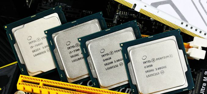
Intel has already started to sell low-power dual-core Core i5/i7 Kaby Lake microprocessors for notebooks, but desktop parts with four cores and high frequencies are due in early 2017, as Intel announced back at IDF and the Kaby Lake-Y/U launch. In advance of the desktop launch, as is typical with how CPUs are launched, Intel has to send out qualification and near-retail samples to partners for pre-testing of release systems. Typically this is kept under wraps, without official public announcements (it's up to you how many of the leaks you want to believe), but late last week Intel sent out a 'Product Change Notification' through its online/public channels, with details about a good portion (no way to tell if it is all the SKUs) of Intel's Core i7 and Core i5-7000 series parts.
Within the PCN, Intel notified its customers about an additional assembly/packaging site for its desktop Kaby Lake-S chips in Vietnam and therefore had to disclose model numbers of the CPUs as well as some of the specifications. In addition, in a separate PCN detailing package adjustments for how chipset ICs are shipped, it would seem that Intel has also mentioned names of its upcoming 200-series chipsets.


According to Intel’s document for partners, the company intends to release at least 11 quad-core processors for desktops based on the Kaby Lake microarchitecture in Q1. What is noteworthy is that the company wants its customers to get ready to receive the first shipments of the KBL-S chips assembled in Vietnam starting from November 4, 2016, this week (which means that the final specs of the new processors have been set and will only be changed in extreme circumstances). The initial KBL-S lineup would seem to include three Core i7 SKUs, seven Core i5 CPUs as well as one Xeon E3 v6 product. (The fact that a Xeon v6 is included in this is interesting, given that Intel removed standard chipset support for Xeon E3 CPUs with Skylake and v5, meaning that both consumer and enterprise platforms are due to land in January.)

All the Kaby Lake-S processors will use the B0 stepping of the core, and will have 100-300 MHz higher base frequency compared to their Skylake-S counterparts. The PCN does not explicitly state the TDP, however we do not expect much to change given the slightly improved 14+ nm technology and the increased frequencies (same thing applies to cache size, which has been consistent for several generations). We have already observed that mobile Kaby Lake CPUs have higher clock rates compared to their predecessors due to enhancements of Intel’s 14+ nm process technology, and we see that their desktop brethren also have improvements on this front. We do not have the final Turbo frequencies at hand, but we expect them to be considerably higher than the base clock rates.
| Basic Specifications of Quad-Core Intel Core i5/i5 and Xeon E3 | |||||||||
| Kaby Lake-S | Skylake-S | ||||||||
| Model | Cores /Threads |
Freq. (Base) |
TDP | Product Code |
S-Spec | Model | Freq. (Base) |
||
| i7-7700K | 4/8 | 4.2 GHz | 95W | CM8067702868535 | SR33A | i7-6700K | 4.0GHz | ||
| i7-7700 | 3.6 GHz | 65W | CM8067702868314 | SR338 | i7-6700 | 3.4GHz | |||
| i7-7700T | 2.9 GHz | 35W | CM8067702868416 | SR339 | i7-6700T | 2.8GHz | |||
| i5-7600K | 4/4 | 3.8 GHz | 95W | CM8067702868219 | SR32V | i5-6600K | 3.5GHz | ||
| i5-7600 | 3.5 GHz | 65W | CM8067702868011 | SR334 | i5-6600 | 3.3GHz | |||
| i5-7600T | 2.8 GHz | 35W | CM8067702868117 | SR336 | i5-6600T | 2.7GHz | |||
| i5-7500 | 3.4 GHz | 65W | CM8067702868012 | SR335 | i5-6500 | 3.2GHz | |||
| i5-7500T | 2.7 GHz | 35W | CM8067702868115 | SR337 | i5-6500T | 2.5GHz | |||
| i5-7400 | 3.0 GHz | 65W | CM8067702867050 | SR32W | i5-6400 | 2.7GHz | |||
| i5-7400T | 2.4 GHz | 35W | CM8067702867915 | SR332 | i5-6400T | 2.2GHz | |||
| E3-1205v6 | ?/? | 3.0 GHz | ? | CM8067702871025 | SR32D | - | - | ||
| Additional Info from Other Sources | |||||||||
| i3-7300* | 2/4 | 4.0 GHz | 65W | ? | SR2MC | i3-6300 | 3.8 GHz | ||
| Pentium G4620* | 2/2 | 3.8 GHz | 51W | ? | SR2HN | Pentium G4520 | 3.6 GHz | ||
| Pentium G3950* | 2/2 | 3.0 GHz | 51W | ? | SR2MU | Pentium G3920 | 2.9 GHz | ||
*CPU details taken from this piece at PCOnline
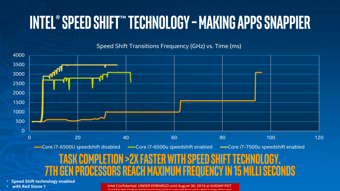
Aside from the 14+ process offering higher frequencies, the base microarchitecture of Kaby Lake-S, as explained at the release of Kaby Lake-Y/U in September, is essentially the same as Skylake. However, on top of increasing the frequencies, Intel is also adding in Speed Shift v2 which allows for much quicker adjustments in CPU frequency over Skylake (down to 10ms rather than 30ms).
It remains to be seen is whether the new 14+ process technology will also enable considerably higher overclocking potential compared to existing CPUs. If it does, then the new chips have a chance to become rather popular among enthusiasts, potentially toppling the i7-2600K as a long term favorite.
It might be noted is that Intel’s Kaby Lake-S will have to compete not only against their predecessors, but also against AMD’s Zen products due in Q1. That being said, some would argue that given AMD's recent presentation of certain benchmark metrics, Zen is geared more towards the high-end desktop crowd. Nevertheless, it looks like early 2017 is going to be an interesting time for microprocessors.
200-Series Chipsets
In addition to model numbers of its Kaby Lake CPUs, Intel also revealed the names of its 200-series chipsets in another document it sent to partners. As expected, the lineup will include the Z270 PCH for enthusiast-class PCs with overclocking capabilities; Q270, H270 and H250 for mainstream systems and B250 for office/business computers.
| Intel 200-Series Chipsets | ||||||
| Name | Socket | Stepping | Product Code | S-Spec | ||
| Intel H270 | LGA1151 | A0 | GL82H270 | SR2WA | ||
| Intel Z270 | GL82Z270 | SR2WB | ||||
| Intel B250 | GL82B250 | SR2WC | ||||
| Intel Q250 | GL82Q250 | SR2WD | ||||
| Intel Q270 | GL82Q270 | SR2WE | ||||
| Intel C422 | LGA1151? | A0 | GL82C422 | SR2WG | ||
| Intel X299 | ?!? | A0 | GL82X299 | SR2Z2 | ||
Also in the list of chipsets were a couple of unknowns as well.
Listed in the PCN is C422, which because it has a 'C' in the name means that this is typically geared towards workstations and Xeon platforms. This may be in line with the E3-1205 v6 CPU SKU as seen in the processor list.
Also is X299, which really throws up a few question marks. The X-series chipsets are typically for Intel's High-End Desktop Platform (HEDT), and we've had X58, X79 and X99 in the last decade, from Nehalem up to Broadwell-E which was released back in May. This means either one of two things - either Intel is bringing the X nomenclature to Kaby Lake, the mainstream platform, or this is the next chipset for HEDT and the future Skylake-E series of processors. The first option in making X299 a Kaby Lake-related platform seems a little odd. However the second one, with Skylake-E, makes sense. After X99, the X119 name doesn't have the same marketability (if Intel was to keep parity with number jumps), but by pushing Skylake-E onto the 200-series naming as X299, it moves both mainstream and HEDT chipset naming strategies onto the same track. Note that we don't have a time-frame for Skylake-E as of yet.
Intel’s motherboard customers, given the Q1 launch, must be ready to receive the 200-series PCH ICs on new reels. According to the PCN, these will come with additional protections bands starting from December 2, 2016. Intel may or may not announce the whole 200-series (not X) lineup at CES, given this late in the day adjustment to core components for the motherboards.
As for improvements of the Intel 200-series chipsets, we are still waiting on official confirmation as to exactly what to expect. Various unconfirmed leaks have indicated additional PCIe 3.0 chipset lanes, some new platform features and support for Intel’s Optane SSDs, however we will be here for the official launch when the time comes. It might be worth noting that almost all the motherboard manufacturers have now formally announced new 100-series BIOS support for Kaby Lake CPUs, meaning not all enthusiasts will have to get new motherboards.


↧
EIZO Launches FlexScan EV2780: 27” 2560×1440 Display with USB Type-C Connector
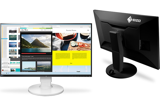
As the USB Type-C connector has become more prevalent, so have devices that support the optional DisplayPort alt mode. To that end, EIZO has introduced their first monitor that users a USB Type-C to connect to host systems. The FlexScan EV2780 is a higher-end office monitor with display features typical of other 27" 1440p monitors, and features thin borders which make the monitor particularly suitable for multi-monitor environments.
The EIZO FlexScan EV2780 is a 27” IPS display with a 2560×1440 resolution, 350 nits brightness, 178° viewing angles, a 60 Hz refresh rate and a 1000:1 contrast ratio. The monitor is aimed at typical home and business applications: it can reproduce 16.77 million colors and supports sRGB color gamut, enough for typical workloads, and has a response time of 5 ms gray-to-gray, enough for mainstream gaming.
One of the key features of the FlexScan EV2780 is its USB Type-C input that works with DisplayPort alternate mode for USB-C. The port can be used to connect various desktops, laptops and smartphones that support DP alt mode for USB-C, including Apple MacBook, Dell XPS 12/13/15, HP Elite X2 1012, HP EliteBook Folio G1, Microsoft Lumia 950/950 XL, LG G5, HTC 10 M10h and so on. The full list of compatible devices can be found at EIZO’s web-site. To ensure compatibility with other modern systems, the FlexScan EV2780 also has a DisplayPort and an HDMI connector in addition to a dual-port USB 3.0 hub.

Another notable feature of the new 27” display from EIZO are its ultra-thin bezels: 1 mm on the sides and top as well as 4.6 mm on the bottom. Since the monitor also has 5.7-mm thick black borders (which results in 6.7 mm borders on sides and top), it cannot be called completely borderless, but its thin frames make it a reasonable candidate for multi-display setups used for business or entertainment purposes. To make it more attractive for such setups, EIZO bundles its proprietary Screen InStyle software that allows users to adjust the color, circadian dimming and power settings on multiple FlexScan displays at once.
| EIZO FlexScan EV2780 | ||
| FlexScan EV2780 | ||
| Panel | 27" IPS | |
| Native Resolution | 2560 × 1440 | |
| Maximum Refresh Rate | 60 Hz | |
| Response Time | 5 ms (gray-to-gray) | |
| Brightness | 350 cd/m² | |
| Contrast | 1000:1 | |
| Viewing Angles | 178°/178° horizontal/vertical | |
| Inputs | 1 × USB Type-C (DisplayPort alt mode) 1 × DP 1.2 1 × HDMI 1.4 1 × DVI-D |
|
| USB Hub | 2-port USB 3.0 hub | |
| Audio | 1 W × 2 audio in/out ports |
|
| Power Consumption | Typical | 11 W |
| Maximum | 96 W | |
Finally, the FlexScan comes with a stand featuring a 155 mm height adjustment, 40° tilt (5° down, 35° up) and 344° swivel & 90° pivot for portrait mode.
EIZO did not reveal MSRP of its FlexScan EV2780 monitor, but an educated guess points towards something around $1000, based on the fact that the company’s previous-gen 27” FlexScan flagship (EV2750) is currently available for $989 at Amazon. Just like other EIZO displays, the monitor comes with with a five-year warranty with a six-month zero bright sub-pixel guarantee.

↧
↧
ARM Announces Mali-G51 Mainstream GPU, Mali-V-61 Video Processing Block
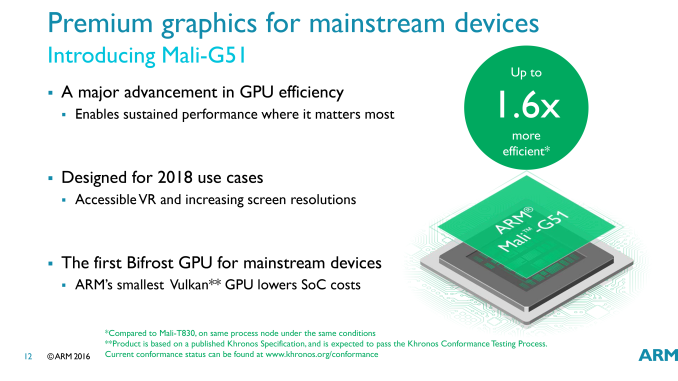
These days ARM and its customers are in the midst of a major evolution in GPU design. Back in May the company announced their new Bifrost GPU architecture, a new and modern architecture for future GPUs. With Bifrost ARM would be taking a leap that we’ve seen many other GPU vendors follow over the years, replacing an Instruction Level Parallelism (ILP)-centric GPU design with a modern, scalar, thread level parallelism (TLP)-centric design that’s a better fit modern workloads.
The first of these new Bifrost GPUs was introduced at the same time, and that was Mali-G71. However as our regular readers likely know, ARM doesn’t stop with just a single GPU design; rather they have multiple designs for their partners to use, running the gamut from high performance cores to area efficient cores. Mali-G71 was the former, and now this week ARM is introducing the latter with the release of the Mali-G51 design.

If Mali-G71 was the successor to the Mali-T880, then Mali-G51 is the successor to the Mali-T820 & T830. That is to say, it’s a mainstream part that has been optimized for performance within a given area – when SoC space and/or cost is at a premium – as opposed to G71’s greater total throughput. Broadly speaking, mainstream parts like Mali-G51 end up in equally mainstream SoCs like the Exynos 7870 (Galaxy A-series), as opposed to flagship-level SoCs like the Exynos 8890 (Galaxy S7). And along those lines, somewhat surprisingly, ARM is rather keen on talking about the VR market in conjunction with G51, even though it’s not their high-performance GPU design. Even G51, they’re confident, can offer good VR performance for the kinds of admittedly simpler workloads they have in mind.
Meanwhile at a technical level, rather than just being a cut-down version of Mali-G71, Mali-G51 is an interesting GPU design in its own right. ARM has opted to go with a continuous development cycle for the Mali-G series, which means that each GPU is in essence branched off of the ongoing Mali design process when a new design is needed. That means besides market-specific optimizations, successive GPUs can contain features not found in earlier GPUs under the same brand, and that’s definitely the case for G51.
So what sets G51 apart from G71? From the area efficiency perspective, the big change here is that ARM has reworked the shader cores to offer what they call a “dual pixel” design, as opposed to G71’s “single pixel’ design. In brief, per a G71 shader core could process 24 FLOPS (12 FMAs) over its three execution engines, while its texture and blending units could process 1 texel and 1 pixel respective. G51, by contrast, has adjusted the throughput ratio to more heavily favor pixel/texel throughput; a G51 shader core has the same 24 FLOPS throughput, but couples that with 2 texels and 2 pixels per clock. ARM did something similar in previous Mali Midgard generations – varying the number of ALUs – and the reason to do so is fairly straightforward, as advanced graphical effects are traditionally more shader-heavy than pixel-heavy. The end result being that for simpler workloads such as application UIs, the need for the shader throughput tends to scale down more rapidly in the mobile space.
| ARM Mali G Series | ||||
| Mali-G71 | Mali-G51 | |||
| Role | High Performance | Area Efficient | ||
| Core Configurations | 4-32 | N/A | ||
| ALU Lanes Per Core (Default) | 12 | 12 | ||
| Texture Units Per Core | 1 | 2 | ||
| Pixel Units Per Core | 1 | 2 | ||
| FLOPS:Pixel Ratio | 24:1 | 12:1 | ||
| APIs | OpenGLES 3.2 OpenCL 2.0 Vulkan |
OpenGLES 3.2 OpenCL 2.0 Vulkan |
||
And while the dual pixel core is the biggest change for G51, it’s not the only change. By being based on a newer iteration of Bifrost, it includes a few notable, low-level tweaks to improve performance. Transcendental performance has been significantly improved; it turns out those operations are still used more often than ARM expected, G51 bakes in better support to maintain higher performance. There are also some outright new instructions on G51, and ARM’s framebuffer compression technology has been improved as well. Version 1.2 of AFBC implements some optimizations for better memory traffic shaping and burst lengths, as well as an improvement for constant color blocks.

Overall, ARM is touting that G51 offers significant improvements to performance, density, and energy efficiency relative to the Mali-T830. On equal processes, G51 a mix of 30% smaller than T830, 60% better performance per mm2, and 60% higher performance per watt. I’m told area efficiency was the primary design in the goal, making the latter a pleasant surprise of sorts.

Finally, like ARM’s other GPU IP announcements, this week’s announcement is about making the technology available to the company’s partners for implementation, rather than being a consumer-oriented announcement. ARM’s partners are already looking at early versions of the G51 design, and based on typical product development cycles, G51 should be showing up in devices in 2018.
Mali-V61
Meanwhile on a quick note, alongside the Mali-G51 GPU, ARM is also announcing the Mali-V61 video processor. This is the product formerly known as Egil, which ARM unveiled back in June while it was still under development. Now, along with G51, V61 is being released to ARM’s partners as well.

V61/Egil has not significantly changed since we’ve last seen it. ARM’s fully modernized video encode and decode block follows a who’s who list of codecs and features, supporting 10-bit HEVC encode/decode and 10-bit VP9 encode/decode. Relative to the VP550 before it, ARM’s latest video processor supports a wider range of codecs, and now, having a full-feature HEVC encoder implementation, offers much better HEVC compression as well.

Ultimately ARM is looking to sell Mali-V61 alongside Mali-G51 and their DP650 display process as a complete graphics solution to partners, which they call the Mali Multimedia Suite (though it can be used stand-along as well). And like Mali-G51, expect to see Mali-V61 start showing up in devices around a year from now.
↧
LaCie Launches 6big and 12big: Up to 60/120 TB External Storage with Thunderbolt 3
LaCie this week has introduced two new workstation-grade external storage solutions using Thunderbolt 3 with the focus on big on-the-desk data storage. The 6big and 12big devices pack in six or twelve enterprise-grade hard drives respectively and can provide up to 60 TB or up to 120 TB of storage space. The HDDs can be implemented as a JBOD or work in various RAID modes. LaCie’s devices promise to be able to take advantage of Thunderbolt 3’s 40 Gb/s bandwidth by providing up to 1400 MB/s or 2600 MB/s read speeds, which can be important for those who work with UHD video content.

The LaCie 6big and 12big DAS with six and 12 drive bays are made of aluminum and come with integrated PSUs and cooling. The storage devices are based on a proprietary platform from LaCie, which supports hardware RAID 0/1/5/6/10/50 modes. Seagate, the owner of the LaCie brand, does not disclose details about the platform behind the new DAS products, but it naturally has a hardware RAID controller (presumably from Seagate’s LSI division) as well as Intel’s Alpine Ridge controller for Thunderbolt 3.

The LaCie 6big and the LaCie 12big external storage devices will be sold in various configurations that use different hard drives, all of which support hot swapping and feature 7200 RPM spindle speed. The top-of-the-range 60 TB and 120 TB models use Seagate’s helium-filled Enterprise Capacity 10 TB HDDs rated for 2 million MTBF and 550 TB/year writes unannounced 10 TB HDD. Meanwhile the lower-capacity DAS devices will use Seagate’s Enterprise NAS HDDs rated for 1.2 million hours MTBF and 300 TB/year writes. The LaCie 6big and 12big will initially be available fully populated, and from a performance point of view maximum read and write speeds will mostly depend on RAID modes.
Update 11/3: As it appears, the LaCie 6big and 12big DAS do not use Seagate's Enterprise Capacity 10 TB HDDs, but rely on unannounced 10 TB drives from the company.
| The LaCie 6big and 12big DAS | |||||
| 6big | 12big | ||||
| HDDs | Unannounced 10 TB HDD Enterprise NAS 8 TB Enterprise NAS 6 TB Enterprise NAS 4 TB |
||||
| Maximum Number of HDDs | 6 | 12 | |||
| Capacity | 60 TB (6 × 10 TB) 48 TB (6 × 8 TB) 36 TB (6 × 6 TB) 24 TB (6 × 4 TB) |
120 TB (12 × 10 TB) 96 TB (12 × 8 TB) 72 TB (12 × 6 TB) 48 TB (12 × 4 TB) |
|||
| RAID | 0/1/5/6/10/50 | ||||
| RAID 0 | Read Speed | 1400 MB/s | 2600 MB/s | ||
| Write Speed | 1400 MB/s | 1700 MB/s | |||
| RAID 5 | Read Speed | 1200 MB/s | 2400 MB/s | ||
| Write Speed | 1150 MB/s | 1200 MB/s | |||
| Ports | 2 × Thunderbolt 3 1 × USB Type-C |
||||
| Fans | 2 | 4 | |||
| PSU | 250 W | 400 W | |||
| Dimensions (W x H x L) | 161 × 225 × 237 mm 6.3 × 8.9 × 9.3 inch |
161 × 447 × 237 mm 6.3 × 17.6 × 9.3 inch |
|||
| Cables Included | USB-C (Thunderbolt 40Gb/s or USB 3.1 10Gb/s) cable USB-C to USB-A cable Power cable |
||||
| Software | LaCie RAID Manager LaCie Private-Public for AES 256-bit software encryption Intego Backup Manager Pro Genie Backup Manager Pro |
||||
| Prices | 24 TB starts at $3199 | 48 TB starts at $6399 | |||
Both DAS solutions from LaCie feature two Thunderbolt 3 ports, making it possible to daisy-chain a display or another TB3 device to the storage arrays. In addition, the 6big and the 12big are equipped with one USB 3.1 Type-C connector which allows to use them with systems not equipped with TB3, but at considerably lower speeds (i.e., up to 350 – 400 MB/s depending on RAID mode).


Like other LaCie’s DAS products with multiple drives, the 6big and the 12big come with the company’s proprietary RAID management software that allows setting them up and then monitoring the condition of the drives.
For pricing the LaCie 6big 24 TB starts at $3199 whereas the LaCie 12big 48 TB starts at $6399.


↧
The Glorious PC Gaming Race GMMK-BRN Modular Mechanical Keyboard Review
In today's review we are taking a look at the GMMK-BRN mechanical keyboard from Glorious PC Gaming Race the first such keyboard from the recently founded US-based company. The minimalistic keyboard features a modular switch design, allowing it to work with the majority of plate-mounted keyboard switches available, regardless of their manufacturer.
↧
Seagate Introduces Game Drive SSD for Xbox (360 and One): 512 GB SSD for $199

Seagate has announced its new Game Drive for Xbox SSD. While the name suggests it is primarily for the original Xbox, this drive is focused for the Xbox One (regular and S) and Xbox 360, allowing users to store more titles using NAND flash memory. Due to the higher performance of SSDs compared to HDDs used in an Xbox One, the Game Drive for Xbox SSD is being promoted as enabling faster boot and game loading times.
The Seagate Game Drive for Xbox SSD has a storage capacity of 512 GB and uses the USB 3.0 interface to connect to the console. According to Seagate, the SSD can store approximately 15 games (assuming that their size is in the range between 35 GB and 50 GB) and various downloadable content. The drive comes in an aluminum enclosure that is durable and somewhat matches the design of the Xbox One (at least, the original black version).
Since the SSD connects to the system using a USB 3.0 Gen 1 cable, its read and write speeds are expected to be limited to near ~400 MB/s (due to overhead incurred by 8b/10b encoding) without additional proprietary drivers (like ASUS' Turbo modes). Nonetheless, 400 MB/s is considerably higher than read/write performance provided by 5400-RPM HDDs used inside the Xbox family (typically, such drives feature read speeds of around 150 MB/s with poor random performance).
Seagate does not disclose whether the Game Drive for Xbox SSD uses TLC or MLC NAND flash, or which controller is in play so, we cannot make any assumptions regarding endurance of the product. Nonetheless warranty times are listed for America (1-year), Europe (2-years) and Asia-Pacific (3-years).
Update 11/3: Seagate confirmed that the Game Drive for Xbox SSD is based on TLC NAND flash. What is more interesting is that Seagate uses an undisclosed controller developed by SK Hynix/LAMD (which probably means that it also uses memory from SK Hynix) along with its own firmware for the drive. In fact, it is highly likely that Seagate uses SK Hynix's Canvas SL301 or SL308 SSD inside its Game Drive for Xbox SSD. We do not know a lot about the SK Hynix SL301, but the SK Hynix SL308 SSD is rated for 150 TBW, which is fairly good for a drive, which will be mostly used for reading, not writing, throughout its lifespan. Even if Seagate's firmware reduces total TBs to be written in a bid to maximize capacity, the endurance of the drive should remain on a decent level (assuming that we are dealing with the SL308).
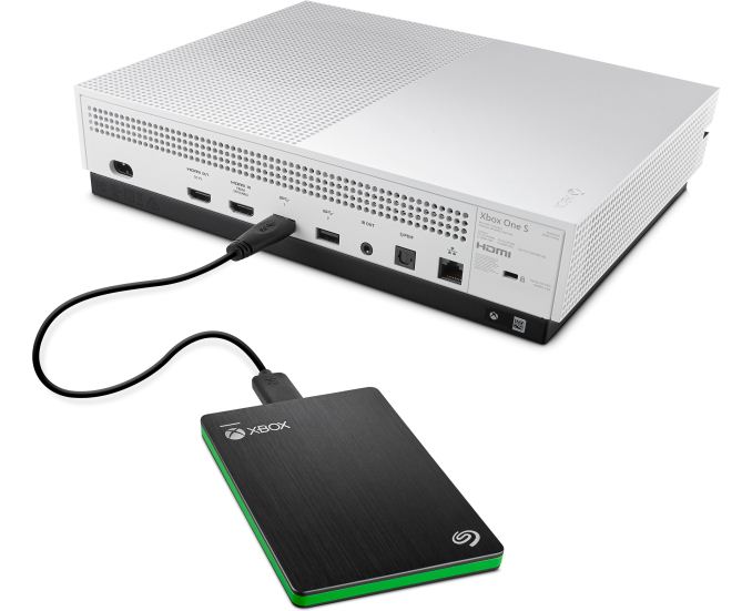
As for pricing, Seagate intends to charge $199.99 for its Game Drive for Xbox SSD, which is $20 to $30 higher compared to other external SSDs compatible with Microsoft’s latest console. Amazon, GameStop and other consumer electronics retailers plan to start selling the device in November.
In addition to the Game Drive for Xbox SSD, Seagate also offers 2 and 4 TB mechanical hard drives for Microsoft’s Xbox One as well as 1 TB SSHD drive for Sony’s PlayStation 4.


↧
↧
Enermax SteelWing Small Form Factor PC Chassis: Aluminum and Glass, $160
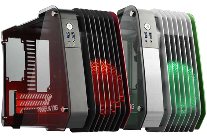
Enermax has started shipments of its new SteelWing chassis this week, designed specifically for small form-factor desktop PCs. The new PC case is made of aluminum and tempered glass, it has an extravagant yet capacious design with advanced ventilation and can fit in a custom liquid cooling system, a high-end graphics card and a powerful processor. The SteelWing is essentially designed to be an aesthetic centerpiece.
The Enermax SteelWing (ECB2010) chassis can accommodate an mATX or a Mini-ITX motherboard, a typical full-height high-end graphics card (up to 290 mm in length), one SFX PSU, as well as two or more 2.5"/3.5" storage devices (one 2.5"/3.5" SSD or HDD can be installed next to the case fan, but only if the space is not used by an LCS radiator). The PC case uses a semi-open design featuring seven aluminum plates as well as one 120-mm fan to ensure proper airflow in the constrained space of the SteelWing. For front panel IO, the case also has two USB 3.0 Type-A ports as well as two 3.5 mm audio jacks on the front panel.

Enermax's press image. That graphics card looks like a banana (says Ian)
Since the PSU is located right next to the CPU, maximum height of the CPU cooler is 80 mm. This limits the choice of the cooling system to either something low-profile (Intel's stock coolers, or something like Noctua’s LH9A), or a sealed liquid-cooling system with a 120-mm radiator (such as the Enermax Liqmax II 120S). Enermax does not impose any limitations for TDP because there is enough space inside the case to house a custom liquid cooling system. As a result, the maximum SFX PSU wattage could be the only limiting factor when it comes to CPU or GPU TDP.
| Enermax SteelWing | ||
| Motherboard Size | Micro-ATX, Mini-ITX | |
| Drive Bays | External | - |
| Internal | Front: 1 × 3.5"/2.5" if the space is not used Rear: 1 × 3.5" and 1 × 2.5" |
|
| Cooling | Front | 1 × 120 mm (included) |
| Rear | - | |
| Top | - | |
| HDD/Side | - | |
| Bottom | - | |
| Radiator Support | Front | Up to 120 mm |
| Rear | - | |
| Top | - | |
| Side | - | |
| Bottom | - | |
| I/O Port | 2 × USB 3.0, 1 × Headphone, 1 × Mic | |
| Power Supply Size | SFX | |
| Dimensions | W: 176 mm × H: 300 mm × D: 387 mm | |
| Colors | Green: ECB2010G Red: ECB2010R |
|
| Features | Glass side panel | |
| Price | $159.99 | |
On the aesthetics end, the Enermax SteelWing has either a green or a red aluminum side panel accompanied by a green or a red 120mm fan. Such styling is clearly made to appeal to performance enthusiasts with a color coded GPU arrangement as well.

Enermax says that the SteelWing chassis are set to be available in the U.S. in the coming days for $159.99 (a tip: first at Newegg).


↧
Microsoft Lifts the Lid on Some Intel Skylake-EP Details via the Open Compute Project
As part of the European Digital Infrastructure Summit in London this week, Microsoft's Azure team will be lifting the lid on Project Olympus, the next generation hyperscale cloud hardware design and model for open source hardware development, in collaboration with the Open Compute Project (OCP). Project Olympus is being described as a way to embrace future platforms in a standardized design, much like other OCP projects, and the open source standards behind the platform are offering insights into Intel’s Skylake-EP Platform, known as Purley.
It seems odd for information about Skylake-EP to be sanctioned at this time (technically none of the documents mention Intel, Skylake or Purley, but it can be deciphered as below), especially given the recent release of Broadwell-E/EP and Intel’s previous stance of limited data release prior to launch. It would appear that the information Microsoft are providing at the summit has been sanctioned, however sometimes putting two plus two together requires a little digging.
All this information is posted on the Microsoft Azure blog, which links directly to the OCP pages where motherboard specifications and server mechanical specifications are provided in PDF format.
It’s a Socket We’ve Seen Before, Which Can Make Waves
Being the motherboard guy at AnandTech, I skipped straight to the motherboard information. Page 31 of the motherboard document gives the following example motherboard drawing:
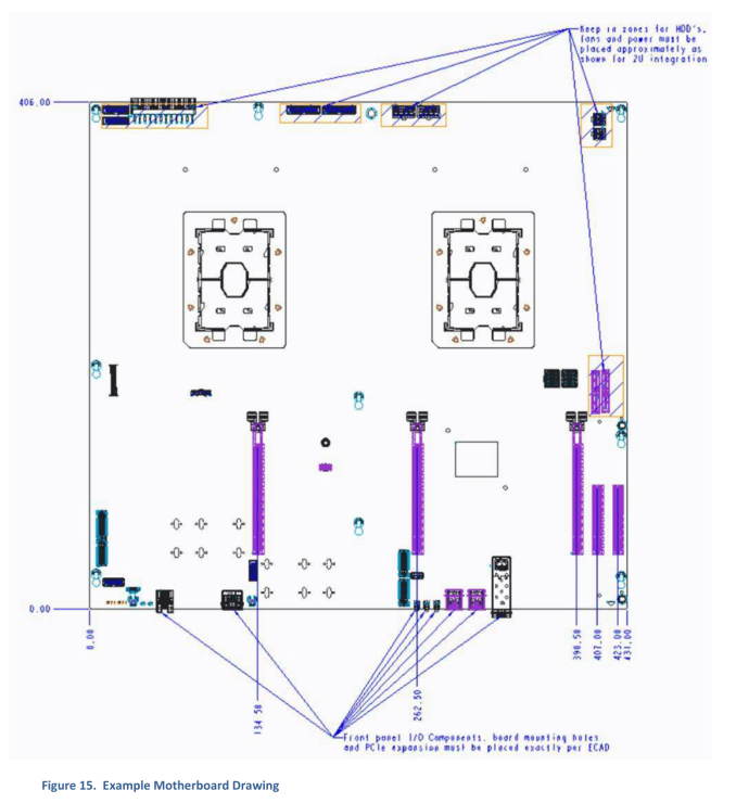
Here is a dual-socket design, with a set of PCIe slots, some power connectors and other I/O components (some fiber Ethernet, for example). But jam packed in the middle are two very large sockets. We’ve seen these before, back at Supercomputing 2015 when Intel announced Knights Landing, which is a Xeon Phi product:
Xeon Phi's Knights Landing design uses an LGA3647 implementation based on its 72 cores, 16GB of MCDRAM, and six memory channels. There are a lot of pins because there’s a lot to power up.
In previous generations of EP processors, both EP and E have shared the same socket. If I wanted to use my E5-2699 v4 Broadwell-EP LGA2011-3 processor in an X99 consumer motherboard instead of an i7-6950X, I could. Essentially all the Core and all the Xeon E5 CPUs have shared a common socket, making it easy for 1P/2P/4P processors to share around. If Purley / Skylake-EP uses the LGA3647 socket, this means one of four things.
The first is that this might not be Skylake-EP, and something odd like Skylake-EN.
The second is that Skylake-E will also share the same socket, and be LGA3647. This sounds somewhat implausible, given that Skylake-EP will have to handle at least the same amount of cores as Broadwell-EP, so there would be a lot of pins on a consumer platform for no reason.
The third possibility is that Skylake-E and Skylake-EP are going to be different sockets. This would indicate a split between consumer HEDT and dual-socket workstations and servers. Given previous generational changes, Skylake-E for consumers is expected to follow a similar pattern – around 2000 pins in a single socket design. However if Skylake-EP is making the jump to a significantly larger socket, especially for 2P workstation and server designs, it will produce a spread of difference in potential for pricing structures and implementation.
The fourth possibility extends from the third, and that Skylake-EP will have two socket designs depending on the size of the core. For Broadwell-EP, there were three designs for the silicon underneath – a low core count (LCC), a medium core count (MCC) and an extreme core count (XCC). If Intel are splitting up the sockets, it may be the case that only the XCC or MCC+XCC sides of the equation are using LGA3647. LCC designs are typically used for the consumer E series parts anyway, so Intel may decide to make the low core designs of EP on the smaller socket. There’s a wealth of possibility here.
I Heard You Like RAM. I Heard You Like Storage.
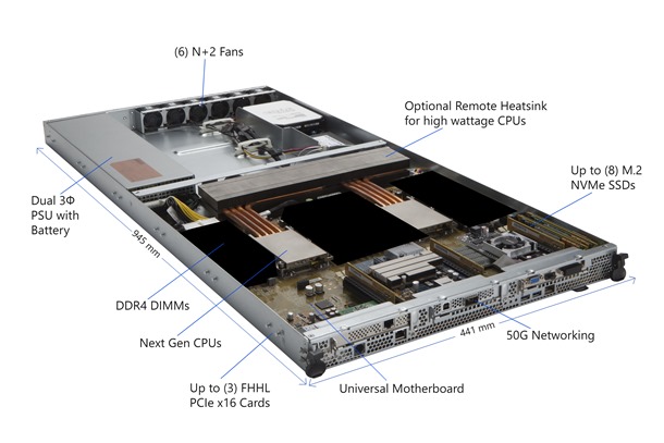
On the main Microsoft Azure page, a handy diagram of an example machine was provided (with some areas blacked out):
Here we see that motherboard from the image above, using two low profile heatsinks with copper piping feeding an optional heatsink inside the chassis. To the sides of each of the sockets are big black squares, indicating where the DDR4 memory should go. Nearer the bottom of the board are networking implementations (50G is labeled), and PCIe slots suitable for three full-height, half-length (FHHL) PCIe cards. Interestingly on the right-hand side, we have labeled ‘up to 8 M.2 NVMe SSDs’.
Back to the motherboard specification, we see the list of blacked out areas along with a more comprehensive sequence of potential configurations:
There are spots for up to 32 DIMMs, which makes 16 per socket. Depending on how many memory controllers the CPU has, this could mean 8-channel and 2 DIMMs per channel (DPC), or 4-channel and 4 DPC. Nowhere does it state the maximum DRAM support per CPU, but DDR4 LRDIMMs are currently at 256GB/module, meaning a potential maximum of 4TB per CPU or 8TB per system. We expect Skylake-EP to support 3D XPoint at some stage as well.
On that list of support also mentions up to 12 SATA devices, up to 3 FHHL cards, and two PCIe x8 slots capable of supporting two M.2 modules each. So this is where that 8x M.2 comes in – if we get four from two PCIe x8 slots, and combine this with up to four M.2 direct attach modules, that makes eight.
The top-level block diagram is also worth a look. Patrick from STH specifically points out the PCIe 3.0 support for the platform:
On the right-hand side, adding up all the PCIe numbers and it comes to 88 PCIe 3.0 lanes, or 44 per CPU. This would be an upgrade on the 40 lanes per CPU currently on Broadwell-EP. There is also provision for PCIe lanes to be used with the mini-SAS connectors on the left-hand side. Technically the BMC also requires a PCIe link as well.
So When?
Given the long product cycles of Intel’s EP platforms, and the fact that the Big Seven cloud providers have a lot of clout over sales means they are most likely testing and integrating the next generation hardware. The release to the public, and smaller players in the OCP space, is a long and slow one. We’re not expecting Skylake-E/EP out until well into 2017, if not the year after, so information will certainly be on the slow burn. Supercomputing 2016 is happening in Utah in a couple of weeks, and although we won’t be there due to scheduling, something may pop out of the woodwork. We’ll keep our eyes peeled.
Source: Microsoft, ServeTheHome


Related Reading
SuperComputing 15: Intel’s Knights Landing / Xeon Phi Silicon on Display
A Few Notes on Intel’s Knights Landing and MCDRAM Modes from SC15
The Next Generation Open Compute Hardware: Tried and Tested
The Intel Xeon E5 v4 Review: Testing Broadwell-EP With Demanding Server Workloads
↧
LaCie Announces Bolt3: 2 TB External SSD at 2.8 GBps over Thunderbolt 3
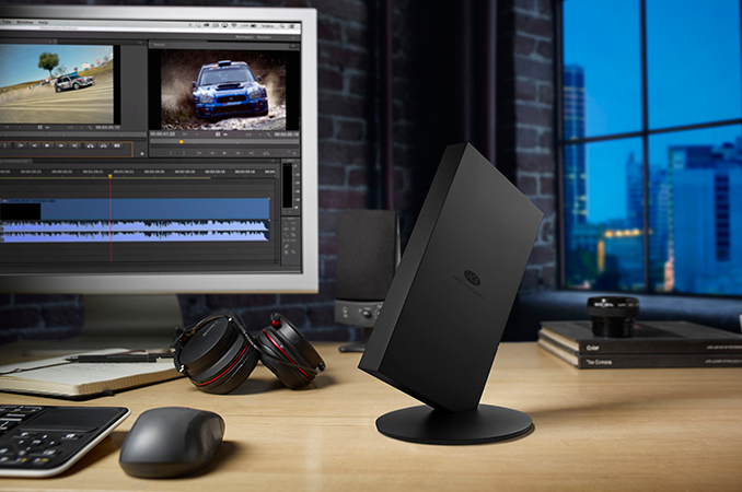
LaCie this week has introduced its first external solid-state storage solution using Thunderbolt. The Bolt3 uses two M.2 SSDs in RAID 0 mode to enable 2 TB of storage as well as up to 2800 MB/s data rate, which is the highest level of performance offered by an available commercial DAS device. The Bolt3 is being advertised for video professionals who edit 4K (and up) video.
The LaCie Bolt3 (STFF2000400) packs in two 1 TB NVMe SSDs in M.2 form-factor that work in RAID 0 mode to enable up to 2800 MB/s read and up to 2200 MB/s write speeds. Seagate, the owner of the LaCie brand, does not disclose which SSDs the device has under the hood, but the company states that the Bolt3 was designed with long-term reliability in mind. This might imply that the device uses drives with high endurance (although, we cannot say whether the maker uses datacenter-grade SSDs). The external storage solution can realize its whole potential when connected to a TB3-enabled computer using the active Thunderbolt 3 cable that is bundled with the device. The Bolt3 also has another TB3 receptacle so to daisy chain more Thunderbolt 3 devices (storage or display) or even charge them (the Bolt3 has its own external PSU).

| LaCie Bolt3 Specifications | |
| STFF2000400 | |
| SSD Model | 2 × SSDs |
| Controller | unknown |
| NAND Flash | MLC NAND |
| Form-Factor, Interface | M.2-2280, PCIe 3.0 x4, NVMe 1.2 |
| Sequential Read | 2800 MB/s |
| Sequential Write | 2200 MB/s |
| Random Read IOPS | unknown |
| Random Write IOPS | unknown |
| Pseudo-SLC Caching | unknown |
| DRAM Buffer | unknown |
| Security | Software-based AES-256 encryption |
| Warranty | 2 years |
| MSRP | $1999 |
From an aesthetic point of view, the LaCie Bolt3 is designed to be seen on a desk. It is made of black aluminum, it features a blue LED on the backside and the enclosure is tilted by 45° to its stand. The mounting mechanism uses neodymium magnets that firmly attach the Bolt3 to its stand, but allow to quickly detach it and transport anywhere. Users can have the drive flat as well. To ensure long-term reliability of SSDs inside, the Bolt3 also has active cooling.
The LaCie Bolt3 belongs to the company’s limited edition series which are designed to promote performance as well as eye-catching design. This means it doesn't come cheap. The LaCie Bolt3 2 TB will be available this quarter for $1999, which is well beyond the price of consumer SSD storage and more than one would have to pay for a DIY 2 TB Thunderbolt 3 external storage solution. As the LaCie Bolt3 is the fastest off-the-shelf external storage solution available today, the manufacturer wants to charge a premium.


↧
ZOTAC Announces VR GO Backpack PC with GeForce GTX 1070
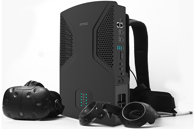
ZOTAC this week has formally introduced its VR GO backpack PC designed for virtual reality enthusiasts. The system is equipped with NVIDIA’s GeForce GTX 1070 graphics, a quad-core CPU from Intel, rich I/O capabilities and a hot-swappable battery. Despite its positioning, the VR GO can be used like a normal desktop computer, which differentiates it from early prototypes of wearable VR PCs from other makers.
ZOTAC is mostly known for its graphics cards and high-performance small form-factor PCs, but not wearable systems (which are not that uncommon: industrial- and even space-grade wearable PCs have existed for years). To develop its VR GO computer, the company had to use experience it obtained from building SFF systems for gamers as well as to find ways to minimize weight and to ensure that the design can handle harsh treatment during gaming sessions. Basically, ZOTAC had to fix everything tightly inside the box while ensuring appropriate cooling and proper position of the I/O ports.
To make it convenient to connect a VR headset to the VR GO, one side of the device has the appropriate ports. The single side has one HDMI output, two USB 3.0 ports and one power connector on top of it. Such positioning greatly simplifies cable management and makes VR gaming with a PC on your back a little more comfortable. The system also comes with a removable battery pack that enables autonomous operation for (waiting on offical numbers) hours.
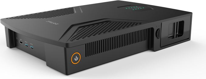
While virtual reality is considered as an important milestone for gaming, it hardly makes sense to develop a PC only for VR, which is why ZOTAC’s VR GO is a powerful PC in general and can be used like a desktop computer too. It has three additional USB 3.0/3.1 Type-A connectors, an SD card reader, four additional display outputs (two HDMI, two DP), two GbE ports as well as two 3.5 mm audio jacks.
Inside the ZOTAC VR GO there is a custom motherboard in a proprietary form-factor carrying an Intel Core i7 CPU, two DDR4 SO-DIMMs, an M.2 SSD (PCIe 3.0 x4), an 802.11ac Wi-Fi module and NVIDIA’s GeForce GTX 1070 MXM module. To cool down the CPU and the GPU (a total TDP of 150 W), ZOTAC uses a proprietary low-profile air cooling system but has not disclosed details. At this point, we do not know whether the manufacturer reinforced the design of its cooler's backplate somehow, but this is a logical thing to expect. To expand the storage capacity of the system, ZOTAC also added one bay for a SATA-based 2.5" storage device (either HDD, which might be affected by rapid movement, or a high capacity TLC SSD).
ZOTAC’s VR GO system is not the first backpack-type PC developed by the company. At Computex 2016 the hardware manufacturer already demonstrated a wearable system, but that was largely a prototype and still in the early design stage. By contrast, the VR GO looks like a commercial product.
ZOTAC does not specify exact availability timeframe for its VR GO backpack PC other than Q4 2016 as well as its estimated price. We expect to see it at CES in early January for sure.


Related Reading
- HP and MSI Demonstrate Backpack PCs for VR Gaming
- ZOTAC ZBOX MAGNUS EN980 SFF PC Review - An Innovative VR-Ready Gaming Powerhouse
- ZOTAC ZBOX CI523 nano Fanless Skylake-U mini-PC Review
↧
↧
Lian Li PC-Q37 Announced: Two-Stage Mini-ITX Chassis with Tempered Glass
On Tuesday Lian Li introduced its PC-Q37 mini-ITX chassis designed for performance and modding enthusiasts based around small-form factor systems. The miniature PC case can accommodate high-end hardware and has two windows to show off custom liquid cooling and lighting effects.
The Lian Li PC-Q37 chassis uses a two-compartment design that allows maximizing cooling and storage capabilities of the system. One of the chambers houses the power supply along with HDDs and/or SSDs, whereas another chamber accommodates the motherboard, graphics card, memory and cooling. In total, the PC-Q37 can fit in three storage devices into a special rack featuring rubber vibration-dampening pads. The case is compatible only with mini-ITX motehrboards but can easily house a high-performance video card that up to 320 mm long (which is slightly longer than contemporary dual-GPU graphics boards) as well as a fairly powerful SFX PSU that is up to 220 mm long and capable of handling high-end hardware.

As for cooling, the Lian Li PC-Q37 supports two 120-mm optional air intake fans on the bottom (or one 140-mm fan), two optional 120-mm exhaust fans on the top as well as two optional 80-mm exhaust fans on the back panel (or you can attach a fourth 2.5” storage device). To protect against dust, the case uses special filters that can be easily removed and cleaned up. The CPU cooler cannot be higher than 130 mm (including fan), but there is plenty of space on top of the chassis to install a radiator of a closed-loop liquid cooling system.
| Lian Li PC-Q37 | ||
| Motherboard Size | Mini-ITX | |
| Drive Bays | External | - |
| Internal | Chamber 1: 1 × 2.5" (only if no 80-mm fans are installed) Chamber 2: 2 × 3.5" and 1 × 2.5" |
|
| Cooling | Front | - |
| Rear | 2 × 80 mm | |
| Top | 2 × 120 mm | |
| HDD/Side | - | |
| Bottom | 2 × 120 mm/1 × 140 mm | |
| Radiator Support | Front | - |
| Rear | - | |
| Top | 2 × 120 mm | |
| Side | - | |
| Bottom | - | |
| I/O Port | 2 × USB 3.0, 1 × Headphone, 1 × Mic | |
| Power Supply Size | SFX | |
| Dimensions | W: 237 mm × H: 345 mm × D: 346 mm | |
| Colors | Grey | |
| Features | Glass front and side panels | |
| Price | $229 | |

On the I/O front, everything is fairly typical for an SFF PC case: the PC-Q37 has two USB 3.0 Type-A as well as two 3.5 mm audio jacks on the front panel.

The Lian Li PC-Q37 should be available shortly at Newegg.com for $229, the company has announced. The price of the chassis is relatively high, but since this is one of a few SFF PC cases designed for performance and modding enthusiasts, its MSRP is not surprising.


Related Reading
- Enermax SteelWing Small Form Factor PC Chassis: Aluminum and Glass, $160
- Cryorig Unveils Mac Pro-Like PC Case for Gaming PCs, Ultra-Slim Desktop Chassis
- Lian Li Launches the PC-A51 ATX Mid-Tower Reverse Air-Flow Chassis
↧
Huawei Munich Press Event Live Blog (starts 2pm CET / 9am ET)
Following the launch of the Kirin 960 SoC, the first announce ARM's Cortex A73 cores and G71 GPU cores, we've been shipped to Munich to discover a new Huawei device (which may or may not have it in). Live blog starts at 9am ET, so tune in then and we'll have the information as it comes through.
↧
Huawei Mate 9 Porsche Design Launched: Curved 5.5-inch 1440p, Kirin 960, 6GB/256GB, $1300, non-US
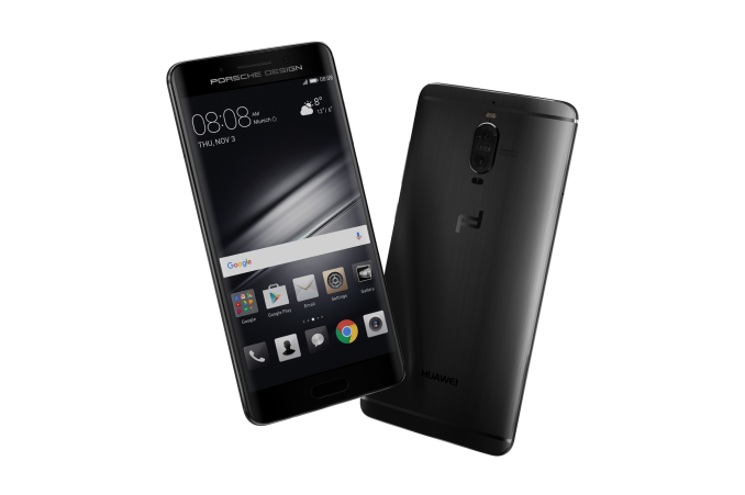
Along with the Mate 9 launch, Huawei's event in Munich today featured a second higher-specification variant with branding tied in with one of the world's premium automobile and design brands. The Mate 9 Porsche Design is a dual-curved 5.5-inch display running a '2K' (2560x1440) resolution smartphone using the latest Kirin 960 SoC, featuring 6GB of DDR4, 256GB of storage via UFS 2.1, and come in at a hefty $1300 price tag. The device is intended for EMEA/APAC markets, not the US.

Despite sharing the Mate 9 name, only a few parts are shared in common between the regular model and the Porsche Design (PD). There's a move down in screen size (5.96in to 5.5in), a curved screen, an increase in resolution (1080p to 1440p), 50% more memory, 2x more storage, and 2x the price. The underlying SoC is the same, as well as battery size, software, audio, fast charging and other features.
| Huawei Mate 9 Series | ||
| Mate 9 | Mate 9 Porsche Design | |
| SoC | HiSilicon Kirin 960 4x ARM Cortex A53 @ 1.8 GHz 4x ARM Cortex A73 @ 2.4 GHz ARM Mali-G71MP8 @ 900 MHz |
|
| RAM | 4 GB LPDDR4-1800 | 6GB LPDDR4 |
| NAND | 64/128 GB UFS 2.1 | 256GB UFS 2.1 |
| Display | 5.96" 1080p LCD | 5.5" 2560x1440p |
| Modem | 2G/3G/4G LTE Cat 12 w/CDMA |
|
| Dimensions | 156.9 (h) x 78.9 (w) x 7.9 (d) mm |
152 (h) x 75 (w) x 7.5 (d) mm |
| Weight | ~190g | 169g |
| Camera | Dual Rear Camera #1 20MP RGB w/OIS, f/2.2 #2 12MP B/W w/EIS, f/2.2 |
|
| Front: 8MP w/AF F/1.9 |
||
| Battery | 4000 mAh | |
| OS | Android 7.0 with EmotionUI 5.0 |
|
| Connectivity | 802.11a/b/g/n/ac 2.4 & 5GHz BT 4.2, GPS/GNSS, DLNA, NFC |
|
| USB | 2.0 Type-C |
3.0 Type-C |
| SIM Size | NanoSIM + NanoSIM (microSD) |
|
| Launch MSRP | 699 Euro | 1359 Euro |
The link up with Porsche, we're told, is more than just a brand. Apparently Porsche are on board with the device design, hardware and software, as well as marketing and distribution (I have a feeling it might be sold alongside vehicles). This is part of Huawei's recent brand strategy, linking devices with known names such as Leica, Harmon/Kardon, and now Porsche to show that it can be a major player in the premium smartphone space. This goes along with their goal to be the #1 smartphone brand in due course.

One thing to note about the Mate 9PE is that the battery is the same as the Mate 9, meaning that at a higher resolution I would expect the battery life of the 9PE to be lower than the 9. With the curved edges, there are more software adjustments that have to be made on top of the OS, which is going to be an interesting look compared to how current curved displays operate. The recent removal of a popular curved smartphone from retail has offered an opportunity that Huawei wants to take to appear as a premium smartphone brand - I'm not necessarily sure a $1300 device is the way to do that, but we will see.
Gallery: Mate 9 Porsche Design![]()
![]()
![]()
![]()
![]()
![]()


↧
Huawei Mate 9 Launch and Hands On: Kirin 960, 5.9in FHD, Daydream VR
Today in Munich Huawei is releasing the covers on their new flagship smartphone. The Mate 9 follows the 8 and 7 as the leading devices under the Huawei brand, each featuring the latest generation HiSilicon Kirin SoC announced at roughly the same time. The SoC in this one is the Kirin 960, as we detailed a couple of weeks ago, and features the first outing of ARM's new Cortex A73 CPU cores as well as the first public implementation of the new ARM Mali-G71 graphics core. Huawei has paired this will an all new CDMA capable Category 12 integrated modem with quad carrier aggregation (4CA) and 4x4 MIMO (at 2CA). The Mate 9 itself is the SoC with an aluminum design with a 5.96-inch Full HD (1920x1080) LCD display, EMUI 5.0, dual Leica rear cameras, and Google DaydreamVR support.
 Nova Plus, Mate 8, Mate 9
As mentioned in our Kirin 960 piece, Huawei (in the Mate 9) is advertising +18% performance on the CPU and +180% on the GPU compared to the Kirin 950 in the Mate 8. The CPU uplift comes from the move to A73 cores over A72, and the GPU is from a doubling from MP4 to MP8 on the GPU along with a new GPU architecture, Bifrost. The CPU and GPU are connected with a new lower power interconnect, ARM's CCI-550, which was promoted as part of ARM's CCI-500 family as offering better efficiency and lower power than the previous generation CCI-400 series. Andrei and Ryan's pieces on both the A73 'Artemis' microarchitecture and the G71 'Bifrost' architectures are well worth the read. For the Mate 9, Huawei is using TSMC's latest 16FFC process - this is a lower cost variant of the original 16FF+ and should be the same 16FFC we see in Apple's A10 cores. Numerous outlets have compared the fact that Huawei is launching a 16nm flagship while others are preparing to launch 10nm devices, however if those are indeed 10nm, Huawei still has 4-5 months (Nov to March) before these devices hit the market and we'll see how they match up in due course.

Nova Plus, Mate 8, Mate 9
Over the past twelve months, the two key devices in Huawei's portfolio have been the Mate 8 and the P9, so naturally one would expect the dual camera feature of the P9 to migrate to the flagship Mate series device. The Mate 9 has two cameras, and rather than using the dual 12MP sensors in the P9, Huawei is using a 20MP black and white camera in one and a 12MP color camera for the other. The color camera will have optical image stabilization, while both with use up to 4K EIS via the internal DSP. With the dual camera design, Huawei is advertising effects such as post processing bokeh, and a 'hybrid 2x zoom' function which crops the 20MP image to a 12MP image to give the effect of zoom. Leica is still practically involved with the branding, apparently assisting with the lenses and the software. Also into the Mate 9 repertoire are a series of effects from previous generations of flagships, such as light painting, but the new device will support Beauty Mode recording and slo-mo recording up to 240fps in 720p/HD mode (although not beauty and slo-mo at the same time). Both rear cameras are set at f/2.2, while the front camera is an 8MP with autofocus and f/1.9.
| Huawei Mate Series | |||
| Mate 7 | Mate 8 | Mate 9 | |
| SoC | HiSilicon Kirin 925 4x A7 @ 1.3 G 4x A15 @ 1.8G T628MP4 @ 0.6G |
HiSilicon Kirin 950 4x A53 @ 1.8 G 4x A72 @ 2.3 G T880MP4 @ 0.9 G |
HiSilicon Kirin 960 4x A53 @ 1.8 G 4x A73 @ 2.4 G G71MP8 @ 0.9 G |
| RAM | 2GB/3GB | 3/4GB LPDDR4 | 4 GB LPDDR4-1800 |
| NAND | 16GB 32GB eMMC 4.0 |
32GB 64GB 128GB eMMC 5.0 |
64 GB 128 GB UFS 2.1 |
| Display | 6" 1080p LCD | 6” 1080p JDI IPS-Neo LCD | 5.96" 1080p LCD |
| Modem | LTE Cat 6 | 2G/3G/4G LTE Cat 6 | 2G/3G/4G LTE Cat 12 w/CDMA |
| Dimensions | 157 (h) x 81 (w) x 7.9 (d) mm |
157.1 (h) x 80.6 (w) x 7.9 (d) mm |
156.9 (h) x 78.9 (w) x 7.9 (d) mm |
| Weight | 185 g | 185g | ~190g |
| Camera | 13 MP f/2.0 1080p30 video |
16MP ( 4608 × 3456 ) Sony IMX298 1/2.8" w/ 1.12µm pixels F/2.0 aperture, ?mm eq. |
Dual Rear Camera #1 12MP RGB w/OIS, f/2.2 #2 20MP B/W w/EIS, f/2.2 |
| 5MP f/2.4 720p video |
Front Facing Camera 8MP ( 3264 × 2448 ) Sony IMX179 1/3.2" w/ 1.4µm pixels F/2.4 aperture, 26mm eq. |
Front: 8MP w/AF F/1.9 |
|
| Battery | 4100 mAh | 4000mAh (15.2 Whr) | 4000 mAh |
| OS | Android 4.2.2 with Emotion UI |
Android 6.0 with EmotionUI 4.0 |
Android 7.0 with EmotionUI 5.0 |
| Connectivity | 802.11a/b/g/n 2.4 & 5 GHz BT 4.0 GPS/GNSS DLNA |
802.11a/b/g/n/ac 2.4 & 5GHz BT 4.2, GPS/GNSS, DLNA, NFC |
|
| USB | 2.0 microUSB | 2.0 microUSB | 2.0 Type-C |
| SIM Size | MicroSIM + NanoSIM (microSD) |
NanoSIM + NanoSIM |
NanoSIM + NanoSIM (microSD) |
| Launch MSRP | 340 Euro | 449-659 Euro | 4GB/64GB: 699 Euro |
For the display, Huawei is promoting a 5.96-inch Full-HD (1920x1080) LED display with a 1500:1 contrast ratio and a tailored '2.5D' glass finish. Color gamut is officially promoted as 96% NTSC. The display will implement the new EMUI 5.0, which as part of our discussions with Huawei's design team is meant to be geared towards ease of use with most applications designed to be 3 clicks away or less. EMUI 5.0 will also feature a new design philosophy centered on blue and white, citing that the minimalist environment and high contrast mirrors a more concise and relaxing user experience. Given Huawei's tendency to ship recent devices with blue screens over the past couple of years (either by chance or design), it seems that blue is here to stay. The Mate 9 does feature a low blue light mode to aid using the device at night, and given previous iterations of this feature it typically adjusts the software LUT and jacks up the greens to give a 'warmer' feel. As a flagship device commanding a flagship price, it will be interesting to see if Huawei has taken steps towards per-unit color calibration similar to its main competitors.
The Mate 9 will be available in two storage variants, either 64GB or 128GB of UFS 2.1, and each device has 4GB of DRAM. In combination with the new version of EMUI, Huawei has promised a lower base for memory occupation (i.e. OS DRAM residency, which seemed oddly high with the Mate 8). For additional storage, the dual Nano-SIM design will allow for a single memory card in the SIM 2 slot, supporting up to 256 GB. Huawei will promote that both SIM slots, depending on the region, will be able to support 4G at the same time, rather than the 4G/GSM combinations in the past. This will be interesting to see the effect on battery life, with the rated 4000 mAh battery.

Nova Plus, Mate 8, Mate 9 (top to bottom)
The 4000 mAh battery is being quoted as an 'all-day' battery, and Huawei is implementing a 'SuperCharge' scheme using an internal controller in both the smartphone and the charging device itself. Rather than the 9V/2A fast charging combinations, Huawei says that SuperCharge uses on-the-fly dynamic voltage adjustments from 3.5-5V with 5A which can offer 3.5 hours of video playback on 10 minutes of charge. As the charger/wallwart being used also has a controller IC implemented, this charging mode can only occur with branded charging devices but this also allows the ICs to communicate regarding temperatures. Charging at high current invariably adds in temperature through losses, and using internal (non-user accessible) phone sensors the temperature of the smartphone can be monitored and charging adjusted as needed. As part of Huawei's presentation, they are stating that the fast charging temperature of the Mate 9 is better than most (if not all) current high-end smartphones on the market today, offering 58% charge in the first 30 minutes as well. Huawei also clarified that no voltage transformation happens on the phone, and cables adhering to the specification will also be required (the controller IC, or 'SuperCharge Processor/SCP', will adjust for the ohmic capacity of the cable). Huawei will also bundle a supercharger for cars as well with the Mate 9.
Connectivity is via a USB 2.0 Type-C connection on the bottom of the phone, and Wi-Fi support is dual-band (2.4 GHz + 5 GHz) 802.11ac 2x2 with Wi-Fi Direct support. This module also supports Bluetooth 4.2 and Low Energy, and with this Huawei is also adding NFC. Next to the Type-C are two speaker grills, and one of the promoted features is the use of four microphones to allow for better recording - one of the promoted software features is a meeting/interview recording mode with various algorithms in place to increase SNR based on input from the various microphones.

Nova Plus, Mate 8, Mate 9
Having used the Mate 8 for at least six months at this point, I can feel it going slower and more antagonizing to switch apps (at times I multitask as if I'm at my desktop). Huawei has recognized that this is one of the pain points when using 'most' devices, so one of the features that Huawei is promoting with the Mate 9 is onboard machine learning, designed to calibrate and optimize the hardware as time goes on to reduce the impact of an aged system. This was described in the form of learning which apps are frequently used and when, and then learning to optimize the storage for contiguous loading as well as prioritize DRAM accesses and CPU instructions for those important apps. Part of this means that applications that have priority will in effect take over up to seven cores on the device, with the remaining cores for background processing. The priority application thus gets more chances to affect the DRAM controller and request storage access, which Huawei says are now also part of the optimization to limit data fragmentation as time goes on and the device is used.
We were able to determine that the machine learning part is both training and inference, and rather than learn through fixed function or specialized hardware, all the computation would be on the cores of the SoC. At present Huawei does all of the analysis on the device, and has not implemented a mechanism for off-site learning or device-to-device learning, in the same way that an autocorrect library might be downloaded to new user devices with certain apps. Thankfully I would expect that the learning and inference of these 'optimization' algorithms is fairly minimal in terms of extra SoC load for day-to-day, so ideally it should not have a hit on battery life.

A well used Mate 8 (left), Mate 9 (right)
On EMUI 5.0 again and Huawei is reintroducing their version of the app drawer to their design. The EMUI 4.1 implementation was distinctly iOS like, with Huawei previously citing that customers enjoyed the design and it provided a combination of ecosystems between available markets. Despite this, customer feedback on an Android device is typically geared towards various features, such as having the app drawer or enabling the ability to have icons for the same app on different home screens. With EMUI 5.0, through the settings, users can enable these features as they won't be the default setting. EMUI 5.0 on the Mate 9 will also still feature all the knuckle gestures and features as in the Mate 8/S and P9, although there is no Force Touch. We were told that EMUI 5.0 has the Force Touch software modules at its core; however it will be up to the device design to support it.
EMUI 5.0 also expands both dual window and dual app sign-in capabilities. Evernote, WhatsApp and Skype will now support dual window, with WhatsApp, Line and WeChat supporting dual-app sign-in. The latter is an interesting implementation allowing users to have two accounts for these messaging applications on the same device, where normally only one is allowed (having a messenger for personal and for work on one device has been regular feedback for Huawei). For upgrading to a new phone, Huawei has also evolved their Huawei Share application allowing users to transfer all contacts, messages and apps directly with phone-to-phone communication rather than via the cloud. It was remarked that Huawei doesn't offer a cloud option, so phone-to-phone is the only way in that regard: Huawei responded saying that cloud is difficult, however the first roll-out of a cloud-based Huawei Share will be in China in the future. There are, as one might expect, inherent country-by-country bylaws with this level of cloud services which Huawei is still in the process of understanding.
Gallery: Mate 9![]()
![]()
![]()
![]()


Huawei will launch the Mate 9 in five colors (region dependent): space gray, moonlight silver, champagne gold, mocha brown and ceramic white. The 4GB/64GB model will retail for 699 Euro.
Hands On
While talking specifications, software and features are interesting (and somewhat easier as a writer), handling a device is a little different. Huawei has kept the curved feel of the Mate series, and to a certain point there is more of a curve to it after some feedback that the Mate 8 was too shallow. As a large smartphone user, I feel having the curved back along with the large screen is a plus - having used the Honor 8 by comparison with its glass rear feels a little odd and uncomfortable. Along with the rear is the fingerprint sensor, which Huawei has made smaller and moved nearer to the cameras.
There are still only five profiles available for fingers for smartphone recognition, which annoys me slightly. I have gotten to the point where I need two fingers on both hands to be registered at different angles, and the Mate 9 will lock the fingerprint sensor after five failed attempts (rather than 10+ on the Mate 8) requiring a PIN to get in. That being said, I can't fault the fingerprint sensor for timing - Huawei has some of the fastest recognition I've seen (even compared to the 6P), which means repeated attempts are fairly quick anyway. The fingerprint sensor now also supports some gestures which can be configured in the settings.
Within the first few moments of handling the device, I did notice a slight design change for the power/reset buttons. On the Mate 8 / Nova Plus / Honor 8, it was always listed as a 'feature' that the power button had a different texture to make it easier to find because both the power/reset buttons were on the same side. With the Mate 9 this feature goes away, leaving two buttons which feel identical aside from their size. I asked Huawei about the reason for the change, but unfortunately I have not had a response yet as to who decided it and why.

As with all new phones, performance in the OS is snappy and seems relatively fluid. As part of the discussions, Huawei was keen to mention that some OS tricks have been employed to improve user experience and the perception of performance though 'non-noticeable' adjustments. I think I spotted one of these - in the gallery app, when scrolling through photographs, in order to avoid a state where the user is scrolling fast and images aren't loading quickly, Huawei will skip a frame or two in the UI to ensure an image preview is always present. To be honest, most phones will skip frames when doing heavy IO processing, so this isn't in itself surprising - but the fact that it is being mentioned as a 'feature' to improve UX is odd. At some point skipped frames for UX will be a thing of the past, though I can see why IO would be an obvious bottleneck.
We've covered features like knuckle gestures and light painting in previous Huawei reviews, and these are also present here. The camera mode on the Mate 9 gets a small revamp, with most features now being offered as slide left/right followed by buttons, rather than a single button for settings. Huawei was keen to promote its new false touching algorithm whereby users might accidentally press the display when taking a photo and draw the focus away. It's a nice feature and somewhat necessary with larger smartphones, and yes it the algorithm isn't fool proof, but I'd like to cite issues I've had with the Mate 8 and false touching when covering events, so even if the algorithm is early stage it can be marked as a positive. I'll leave the smartphone dual camera analysis for Matt's full review of the device, but I can confirm it takes pictures.
Some of Huawei's claims will be difficult to test in a full review, such as the long-term performance metric gathering, purely because of the time required and the need for a baseline on the same device receiving the same application profile trace. However, the A73/G71 combination in the SoC is going to be an expected performance matchup through 2017, and we'll be keen to see how the updated custom cores from the other major smartphone manufacturers shape up. If we get time with a device after the announcement, I'll try and run some basic benchmark numbers.
↧
↧
AnandTech Call for Writers: 2016
The Call for Writers has become something of an annual tradition over here at AnandTech. As anyone who follows the site knows very well, the list of things we have to review/cover usually exceeds our available time. So the call for writers gives us a chance to find new talent and new opportunities to grow, be it into new coverage areas entirely or just covering more of the existing products our readers have come to enjoy over the years.
The ultimate purpose of the Call for Writers is to find new talent. To continue to grow and improve our content, we need your help. We're looking for writers with a true passion for the technology we cover, a deep understanding of what's out there and a thirst for more knowledge.
We're looking for contributors to help out both with reviews as well as our short to medium form Pipeline coverage. The areas in particular we're looking for help with are listed below:
- News/Pipeline (US & Euro)
- Systems/Laptops (US-only)
- GPUs (US-only)
- Mobile/Smartphones
- Wearables
- Podcast Editor
- Networking
- Memory
- Monitors
- Home Automation/IoT
- Professional Graphics/GPU
If you find yourself at the intersection of knowledge and passion about any of those areas, and have some time to contribute, you're exactly what we're looking for. These are paid, part-time positions that we're looking to fill, with most positions open on a world-wide basis, and certain positions primed for a quick promotion to full-time. What I need is a writing sample that demonstrates your ability to talk about any one of these topics. Your sample can be in the form of a review, a pipeline post or an analysis piece - it should be something that looks like it would fit in on AnandTech.
Once you've produced it, send it on over to callforwriters@anandtech.com. Please also include a description of what subject(s) you would be interested in writing about, and some basic information about your background and where you're located. We'll read through all samples but can't guarantee a reply due to the sheer volume of submissions we tend to receive. If we like what you've sent and there's a potential fit on the team, we'll be in touch.
I'll conclude this post with a passage from our About page:
In the early days of technology reporting on the web the focus was almost exclusively on depth. We had a new medium for content that didn't come with the same restrictions as more traditional forms. We could present as much data as we felt was necessary and we could do it quicker.
As the web grew, so did the approach to gaining readership. In many cases, publishers learned from the tips and tricks of more traditional media to growing their audience. The focus shifted away from ultimate understanding of what was being reported, to producing content significantly motivated by increasing traffic, or revenue, or both. Thorough observations were out; sensationalism, link baiting, and the path to shallow 10-o'clock-news reporting were in.
While I believe it's definitely easier to produce content by going this route, I don't believe it's the only way to build a well read website.
If the above resonates with you and you'd like to help by being a part of something different, I'd encourage you to submit a writing sample.
Frequently Asked Questions
Q: How old do I need to be to work for AnandTech?
A: You need to be old enough to legally work in your country of residence without significant restriction. Otherwise we have no specific requirements so long as you can do the job well. Anand started the site at 14, after all...
Q: Do I need to be located in the United States to work for AnandTech?
A: Some positions do require that you be in the US for logistical reasons, and those specific positions are noted. However unless otherwise noted, most positions are open on a world-wide basis.
Q: Do I need to supply my own products for testing or contacts at companies? (i.e. do I need to be an insider?)
A: No. Assuming for the moment you have a computer to write on, then you already have the most important piece of equipment that you need. Meanwhile you will need some knowledge of the field at hand, but we will introduce you to the people you need to know for your position at AnandTech.
Q: Can I really work for AnandTech even though I don't have a Ph.D in electrical engineering?
A: Yes! We are first and foremost looking for people with a passion to learn, and the knack to make it happen. There's a certain degree of baseline knowledge needed for any given position, but if you can read existing AnandTech articles then you're already half-way there.
Q: Is there a submission deadline?
A: We have a tentative end point for the middle of November.
↧
ZOTAC ZBOX MAGNUS ERX480: SFF PC with Intel Core i5, AMD Radeon RX480, USB-C
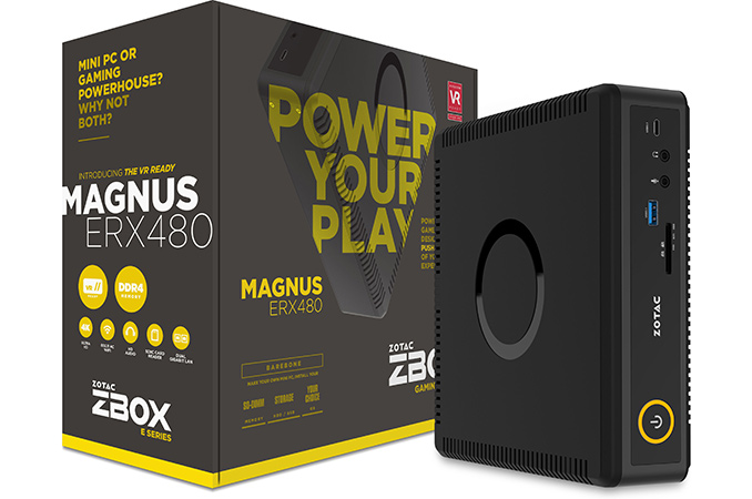
ZOTAC has introduced a new small form-factor system that integrates AMD’s Radeon RX 480 graphics as well as an Intel quad-core Core i5-6400T. The compact PC is designed to drive up to four 4K displays at once and can be used both for gaming as well as for productivity applications that demand multiple monitors. In fact, the manufacturer officially positions the system as an entry-level machine for VR gaming.
The ZOTAC ZBOX MAGNUS ERX480 PC is powered by Intel’s Core i5-6400T processor (4C/4T, 2.2 GHz/2.8 GHz, 6 MB LLC cache, 35 W TDP) as well as a custom LGA1151 motherboard with two slots for DDR4-2133 SO-DIMM memory. AMD’s Radeon RX480 MXM module, one M.2-2280 slot for a SATA SSD, a SATA connector, two Gigabit Ethernet controllers, a 802.11ac Wi-Fi/BT 4.2 module and a USB 3.1 controller make up the other key features.

When it comes to connectivity, the ZBOX MAGNUS ERX480 is an example of reasonable set of I/O ports. The system features two HDMI 2.0, two DisplayPort 1.3, two GbE, two 3.5mm audio, two USB 3.0, two USB 2.0, one USB 3.1 Gen 2 Type-A and one USB 3.1 Gen 2 Type-C connectors. In addition, the PC has a 3-in-1 card reader (SD/SDHC/SDXC UHS II). Users with 5.1- or 7.1-channel speaker systems will have to use an external USB audio solution however.

From performance point of view, the ZBOX MAGNUS ERX480 meets the minimum requirements that Oculus VR set for games compatible with the Oculus Rift VR headset back in the first half of 2015: it has a quad-core CPU along with AMD’s Radeon RX 480 GPU, supports up to 32 GB of DDR4 memory and can be equipped with 2 drives (1x M.2 and 1x 2.5"). If game developers follow recommendations of Oculus VR, the MAGNUS ERX480 should run VR titles for Oculus VR with decent framerate.
| ZOTAC ZBOX MAGNUS ERX480 Specifications | |||
| ZBOX MAGNUS ERX480 (barebones) |
ZBOX MAGNUS ERX480 PLUS (w/ DRAM+M.2) |
ZBOX MAGNUS ERX480 WINDOWS (w/ DRAM+M.2) |
|
| CPU | Intel Core i5-6400T (4 cores, 2.2 GHz/2.8 GHz, 6 MB LLC, 35 W) | ||
| PCH | unknown 100-series | ||
| Graphics | AMD Radeon RX480 at 1050 MHz: 2304 stream processors 144 texture units 32 ROPs 256-bit memory interface 4 GB of GDDR5 7 GT/s memory |
||
| Memory | Two SO-DIMM slots, up to 32 GB of DDR4-2133 | 8 GB of DDR4-2133 (one module) | |
| Storage | M.2 SATA 1x SATA 6 Gbps 2.5" |
120 GB M.2 SATA SSD 1 TB 2.5" HDD |
|
| Wi-Fi | 802.11ac + BT 4.2 | ||
| Ethernet | Two Gigabit Ethernet with RJ45 connector | ||
| Display Outputs | 2 × HDMI 2.0 2 × DisplayPort 1.2 |
||
| Audio | 3.5 mm audio in and audio out | ||
| USB | 2 × USB 2.0 Type-A (480 Mbps) 2 × USB 3.0 Type-A (5 Gbps) 1 × USB 3.1 Type-A (10 Gbps) 1 × USB 3.1 Type-C (10 Gbps) |
||
| Other I/O | 3-in-1 card reader (SD/SDHC/SDXC UHS II) | ||
| Dimensions | 210 mm × 203 mm × 62.2 mm 8.27 × 7.99 × 2.45 inches |
||
| PSU | External | ||
| OS | - | Windows 10 Home | |
Speaking of dimensions, it should be noted that like other MAGNUS-series PCs, the ERX480 is not as tiny as Intel’s NUC, but it is not as large as some other models in Zotac's lineup. The relatively small size of the new compact PC from ZOTAC is a result of the company’s decision to use relatively low-power components (the manufacturer claims that the power draw of the ERX480 is 160 W) and air-cooling. We do not know whether the PC gets noisy under high loads, but this is a possibility as the system uses two blowers.
ZOTAC traditionally plans to offer three versions of the MAGNUS ERX480: a barebones with just the CPU and GPU installed; a Plus version with a 8 GB DDR4 memory module, a 120 GB SATA M.2 SSD as well as 1 TB HDD; and a Windows edition with DRAM, storage and Windows 10 Home operating system pre-installed. The manufacturer does not disclose its MSRPs at this time, but claims that all the PCs will be available by the end of November.


Related Reading:
↧
ADATA Ultimate SU800 SSDs in M.2 Announced: Entry-Level 3D NAND SSDs for Laptops
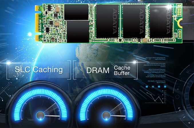
This week ADATA expanded the lineup of its SSDs featuring 3D NAND memory by announcing its Ultimate SU800 drives in an M.2 form-factor. The new SSDs offer similar performance and features as the 2.5” Ultimate SU800 drives introduced earlier this year, hence, the key selling points of the newcomers is their relatively affordable price as well as compatibility with ultra-thin notebooks.
The ADATA Ultimate SU800 family of M.2 SSDs include models with 128 GB, 256 GB, 512 GB and 1 TB capacity (the largest one will hit the market a bit later than the others — it is not even listed on the manufacturer's web-site yet). Just like their 2.5-inch brethren, the new drives are based on Silicon Motion’s SM2258 controller (which has four NAND flash channels and LDPC ECC technology) as well as 3D TLC NAND flash memory produced by IMFT. The Ultimate SU800 M.2 SSDs use a SATA 6 Gbps interface and support a DRAM buffer as well as pseudo-SLC caching to maximize the writing speed of the drives.
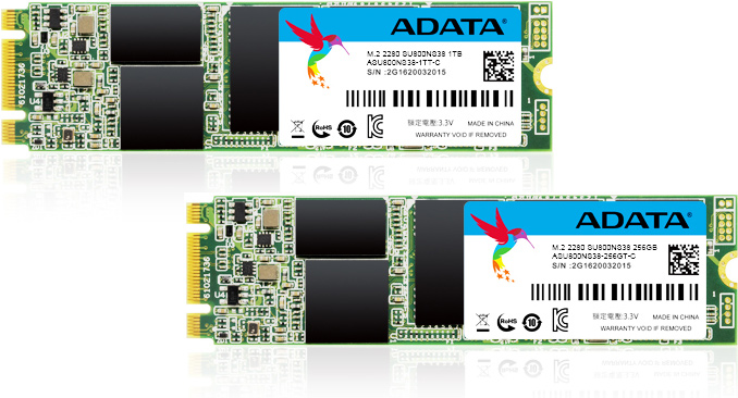
Speaking of performance, ADATA claims that the higher-capacity Ultimate SU800 SSDs feature up to 560 MB/s read and up to 520 MB/s write speed, whereas the 128 GB model is a bit slower when it comes to writing (up to 300 MB/s). ADATA does not mention random performance of the SSDs as well as their power consumption, but the SM2258 controller in other devices is capable of up to 90,000 read IOPS and up to 80,000 write IOPS, which is good enough for client storage devices.
| ADATA Ultimate SU800 M.2 Specifications | ||||
| Capacity | 128 GB | 256 GB | 512 GB | 1 TB |
| Model Number | ASU800NS38- 128GT-C |
ASU800NS38- 256GT-C |
ASU800NS38- 512GT-C |
ASU800NS38- 1TT-C |
| Controller | Silicon Motion SM2258 | |||
| NAND Flash | 3D TLC NAND | |||
| Sequential Read | 560 MB/s | |||
| Sequential Write | 300 MB/s | 520 MB/s | ||
| Random Read IOPS | Up to 90K IOPS | |||
| Random Write IOPS | Up to 80K IOPS | |||
| Pseudo-SLC Caching | Supported | |||
| DRAM Buffer | Yes, capacity unknown | |||
| TCG Opal Encryption | No | |||
| Power Management | DevSleep | |||
| Warranty | 3 years | |||
| MTBF | 2,000,000 hours | |||
| MSRP | $69.99 | $84.99 | $149.99 | unknown |
Since 3D NAND is made using larger process technologies than planar NAND flash memory, it naturally has better endurance and higher performance, which is why ADATA declares 2 million hours MTBF for its Ultimate SU800 M.2 SSDs, which is 0.5 million hours higher compared to 2D NAND-based drives. Nonetheless, the warranty period for the new storage devices is standard - three years.
Meanwhile, prices of the Ultimate SU800 M.2 SSDs are $5 to $10 higher compared to the same products in a 2.5-inform-factor. ADATA plans to charge $69.99, $84.99 and $149.99 for 128 GB, 256 GB and 512 GB versions of its Ultimate SU800 SSDs. Since the new drives offer higher endurance and better performance than their predecessors, ADATA positions them above the existing TLC-based M.2 SSDs and reflects this in MSRPs. Eventually, the new drives will inevitably get more affordable, but today the manufacturer charges a small premium for 3D NAND-powered SSDs.


Related Reading:
↧