Western Digital has a number of direct-attached storage (DAS) products based on hard drives. They cater to different market segments. These DAS units usually employ a USB port to connect to the host (Thunderbolt is also popular in the high-end market). Within the USB storage bridge market segment, Western Digital has a number of product lines tuned to specific use-cases. For example, the My Passport product line focuses on striking a balance between capacity and portability, while the My Book targets a 'desktop' use-case with external power, but much higher capacity. Today, we will be taking a look at the 2016 redesign of the My Book and My Passport units.
↧
Western Digital My Book 8TB and My Passport 4TB External HDDs Review
↧
Samsung Foundry Announces 10nm SoC In Mass-Production
![]()
Today Samsung announced mass production of a SoC built on its third-generation 10nm "10LPE" manufacturing node. It was only this January that Samsung announced mass production of its 14LPP process that ended up being used in the Exynos 8890 and the Snapdragon 820 powering up a large amount of flagship devices this year.
This time around the announcement comes quite early compared to the past 2 years and I wasn't expecting any news from the foundry till maybe later in the quarter. This does however bode well for the SoCs built on the process as they seem they'll be able to easily make the spring 2017 device release schedule.
There wasn't any specification as to what kind of SoC the mass production announcement is refering to, but it's very likely we're talking about S.LSI's next generation Exynos - or maybe even Qualcomm's Snapdragon 820 successor, both of which we'll hopefully hear official announcements from in the coming months.
Samsung’s new 10nm FinFET process (10LPE) adopts an advanced 3D transistor structure with additional enhancements in both process technology and design enablement compared to its 14nm predecessor, allowing up to 30-percent increase in area efficiency with 27-percent higher performance or 40-percent lower power consumption. In order to overcome scaling limitations, cutting edge techniques such as triple-patterning to allow bi-directional routing are also used to retain design and routing flexibility from prior nodes.

Credit: DAC 2016 Samsung/Synopsys Breakfast - Ready to Design at 10nm!
The process promises some significant speed and power efficiency advantages over current generation designs so it's likely the next generation of devices will see a large boost, similarly to how the first 14/16 SoCs had large improvements over previous generation 20/28nm designs.
Interestingly the new SoCs will have an edge on recent and upcoming designs still being released on 16nm manufacturing processes, such as Apple's A10 or other TSMC customers who have to wait till next year for 10FF. This presents itself as an opportunity for vendors such as Samsung and Qualcomm to try to close the performance and efficiency gap seen in the current generation through the manufacturing process' good timing.
↧
↧
The GIGABYTE X170-Extreme ECC Motherboard Review: For When Skylake Xeons need SLI and Thunderbolt 3
When we reviewed the GIGABYTE MW31-SP0, I stated at the time that due to the design of many of the Xeon focused motherboards, only two or three were actually geared up for SLI certification. It comes down to the motherboard implementing the C236 chipset (over the C232) and the manufacturer providing an x8/x8 PCIe lane allocation and actually going for certification. The reality seems to be that not that many Xeon users want/need SLI for gaming, hence the low number of products available. But GIGABYTE aims for the X170-EXTREME ECC to be the best motherboard on the market for just such an occasion, while bundling Thunderbolt 3 support as well.
↧
Qualcomm Announces New X50 5G Modem, First Gigabit Class LTE Network and Router
![]()
Qualcomm made three announcements about connectivity products today at it 2016 4G/5G Summit in Hong Kong. The first announcement, aimed at easing the transition between the 4G LTE networks we have today and the 5G networks of the future, is a partnership with Netgear, Telstra, and Ericsson to deliver the first commercial gigabit class LTE device and network. Qualcomm sees gigabit LTE as a necessary building block and foundation for 5G, providing more bandwidth over a wider area until even higher bandwidth, shorter range 5G networks come online. Telstra, an Australian telecommunications provider, is currently building and testing the first gigabit LTE network, with equipment and software from Ericsson, in a bid to bring higher bandwidth internet access to the home without the expense of laying fiber cables.
Telstra is pushing for a commercial launch in the next few months and will be providing its customers with the new Netgear Mobile Router MR1100—a gigabit LTE endpoint and Wi-Fi router that delivers up to 1Gbps download speeds through a combination of 3x carrier aggregation, MIMO technology (4x4 MIMO on two aggregated carriers plus 2x2 MIMO on the third carrier), and 256-QAM modulation. Inside is a Qualcomm Wi-Fi solution and Qualcomm’s Snapdragon X16 LTE modem paired with Qualcomm’s WTR5975 RF transceiver.
This is the Snapdragon X16’s first appearance after it was unveiled back in February of this year at Qualcomm’s annual Analyst Day. The X16 is a sixth-generation discrete LTE modem manufactured on a 14nm FinFET process that’s capable of 1Gbps (Category 16) on the downlink and 150Mbps (Category 13) on the uplink. According to Qualcomm:
The Snapdragon X16 LTE modem is designed to reach Gigabit Class LTE speeds using the same amount of spectrum as Category 9 LTE devices. By using carrier aggregation and 4x4 MIMO, the Snapdragon X16 LTE modem can receive 10 unique streams of data using only three 20 MHz carriers. Its support for 256-QAM boosts the peak throughput of each stream from ~75 Mbps to ~100 Mbps, with additional gains possible with modem data compression. Additionally, with support for Licensed Assisted Access (LAA) as well as LTE-U, this combination reduces the amount of licensed spectrum required—to 40 MHz or less—to vastly expand the number of operators that can deploy Gigabit Class LTE speeds around the globe.
The X16 LTE modem will find a home integrated inside the next, currently unnamed, Snapdragon SoC, which is the second big announcement today. This next generation SoC will be powering flagship phones in 2017, enabling faster download speeds as carriers begin rolling out gigabit capable networks over the next 12 months, according to Qualcomm.
The final big announcement is Qualcomm’s first 5G modem, the Snapdragon X50. Designed to work only in the 28GHz millimeter-wave spectrum initially (supporting the Verizon 5GTF and KT 5G-SIG specifications), it’s capable of 8x100MHz carrier aggregation, giving it access to 800MHz of spectrum versus 80MHz (4x20MHz) for Qualcomm’s X16 LTE modem. All of this extra bandwidth enables up to 5Gbps on the downlink.
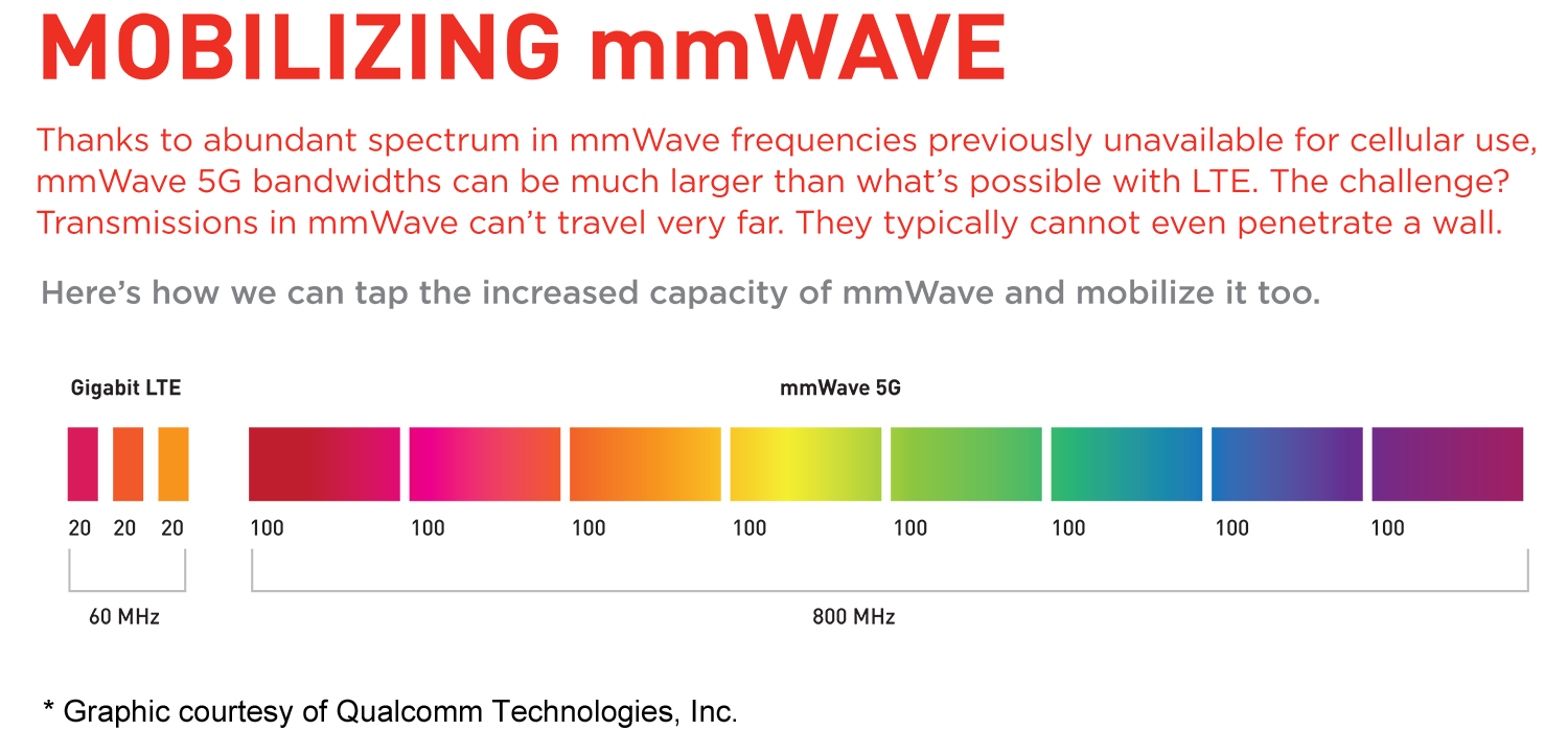
The downside to using higher frequencies, however, is their limited penetration and range. Qualcomm looks to mitigate these issues by using an array of many small antennas and employing adaptive beamforming and beam tracking to enable non-line-of-sight operation, essentially using surface reflections to see around corners and objects.
The Snapdragon X50 5G modem will be paired with two of the new SDR051 millimeter-wave transceivers and the PMX50 power management IC to support fixed wireless applications or future mobile devices. Because it only supports millimeter-wave frequencies, it needs to be paired with an additional 4G LTE modem to provide data uplink and voice capabilities and to allow seamless handoff between 4G and 5G networks depending on availability.
Qualcomm expects the Snapdragon X50 to begin sampling in the second half of 2017, with the first commercial products incorporating the new components showing up in the first half of 2018.
↧
Qualcomm Announces Snapdragon 653, 626, & 427 SoCs: Include X9 LTE Modem and Support for 8GB RAM
![]()
Today at Qualcomm’s 2016 4G/5G Summit in Hong Kong, the company announced several new additions to its low- and mid-tier Snapdragon SoC lineup, including the Snapdragon 427, 626, and 653. Each new Snapdragon SoC builds on its predecessor, adding a few key features.
The new Snapdragon 653 is the “Pro” version of the existing 652 similar to how the Snapdragon 821 is a “Pro” version of the 820. Qualcomm raised the max frequency of the Snapdragon 653’s four ARM Cortex-A72 CPUs to 1.95GHz, up from 1.80GHz in the 652, but kept the max frequency of the four ARM Cortex-A53 CPUs the same. There’s still an Adreno 510 GPU in the new SoC, but its peak frequency has also been increased.
The Snapdragon 653 still uses LPDDR3-1866 memory with 14.9GB/s of bandwidth like the 652, but doubles the amount of addressable RAM from 4GB to 8GB. This is a prudent extension given the current trend towards 4GB and 6GB configurations for Android phones in the mid-range segment and flagship phones pushing towards 8GB.
The Snapdragon 653 also received a modem upgrade: The Snapdragon X9 LTE modem replaces the Snapdragon X8 LTE modem in the 652. The X9 still supports up to 300Mbps on the downlink using 2x20MHz carrier aggregation and 64-QAM (Category 7), but boosts the uplink to 150Mbps by adopting 64-QAM (Category 13). The X9 can also improve call clarity when using the Enhanced Voice Services (EVS) codec for VoLTE calls.
| Qualcomm Snapdragon Mid-Range to High-End SoCs | ||||
| SoC | Snapdragon 650 (MSM8956) |
Snapdragon 652 (MSM8976) |
Snapdragon 653 (MSM8976 Pro) |
Snapdragon 820 / 821 (MSM8996 / MSM8996 Pro) |
| CPU | 2x Cortex-A72 @ 1.80GHz 4x Cortex-A53 @ 1.44GHz |
4x Cortex-A72 @ 1.80GHz 4x Cortex-A53 @ 1.44GHz |
4x Cortex-A72 @ 1.95GHz 4x Cortex-A53 @ 1.44GHz |
2x Kryo @ 2.15GHz / 2.34GHz 2x Kryo @ 1.59GHz / 2.19GHz |
| GPU | Adreno 510 | Adreno 530 @ 624MHz / 653MHz | ||
| Memory | 2x 32-bit @ 933MHz LPDDR3 14.9GB/s |
2x 32-bit @ 1866MHz LPDDR4 29.9GB/s |
||
| ISP/Camera | Dual ISP 21MP |
Dual 14-bit Spectra ISP 25MP / 28MP |
||
| Encode/Decode | 2160p30, 1080p120 H.264 & H.265 |
2160p30 (2160p60 decode), 1080p120 H.264 & H.265 |
||
| Integrated Modem | Snapdragon X8 LTE (Category 7) DL = 300Mbps 2x20MHz CA, 64-QAM UL = 100Mbps 2x20MHz CA, 16-QAM |
Snapdragon X9 LTE (Category 7/13) DL = 300Mbps 2x20MHz CA, 64-QAM UL = 150Mbps 2x20MHz CA, 64-QAM |
Snapdragon X12 LTE (Category 12/13) DL = 600Mbps 3x20MHz CA, 256-QAM UL = 150Mbps 2x20MHz CA, 64-QAM |
|
| Mfc. Process | 28nm HPm | 14nm LPP | ||
* Snapdragon SoCs still in production but not shown: 810, 808, 805, 801, 800
The Snapdragon 625 gets a new “Pro” version too in form of the Snapdragon 626. Both of the Cortex-A53 CPU clusters get a boost from 2.0GHz to 2.2GHz, but Qualcomm did not disclose the frequency of the Adreno 506 GPU.
The Snapdragon 625’s X9 LTE modem carries over to the 626, but the new SoC updates Bluetooth support from 4.1 to 4.2. The Snapdragon 626 also supports Qualcomm’s TruSignal antenna boost technology, which optimizes reception in weak signal strength conditions and from the attenuation that occurs when holding a phone. Working together with the antenna matching tuner (a separate IC that’s part of Qualcomm’s RF360 suite) and transceiver, the X9 LTE modem in the Snapdragon 626 performs the processing that enables the dynamic tuning.
| Qualcomm Snapdragon Mid-Range SoCs | ||||
| SoC | Snapdragon 615 / 616 (MSM8939) |
Snapdragon 617 (MSM8952) |
Snapdragon 625 / 626 (MSM8953 / MSM8953 Pro) |
|
| CPU | 4x Cortex-A53 @ 1.70GHz 4x Cortex-A53 @ ? |
4x Cortex-A53 @ 1.50GHz 4x Cortex-A53 @ ? |
4x Cortex-A53 @ 2.00GHz / 2.20GHz 4x Cortex-A53 @ 2.00GHz / 2.20GHz |
|
| GPU | Adreno 405 | Adreno 506 | ||
| Memory | 1x 32-bit @ 800MHz LPDDR3 6.4GB/s |
1x 32-bit @ 933MHz LPDDR3 7.46GB/s |
||
| ISP/Camera | 21MP | Dual ISP 24MP |
||
| Encode/Decode | 1080p30 H.264 / 1080p60 H.264 & H.265 |
2160p30 H.264 & H.265 |
||
| Integrated Modem | Gobi 4G LTE / Snapdragon X5 LTE (Category 4) DL = 150Mbps 1x20MHz CA, 64-QAM UL = 50Mbps 1x20MHz CA, 16-QAM |
Snapdragon X8 LTE (Category 7) DL = 300Mbps 2x20MHz CA, 64-QAM UL = 100Mbps 2x20MHz CA, 16-QAM |
Snapdragon X9 LTE (Category 7/13) DL = 300Mbps 2x20MHz CA, 64-QAM UL = 150Mbps 2x20MHz CA, 64-QAM |
|
| Mfc. Process | 28nm LP | 14nm LPP | ||
The Snapdragon 427 (MSM8920) is the newest member of the lower-tier 400 series, which now encompasses seven Snapdragon SoCs (400, 412, 415, 425, 427, 430, 435), ranging from the Snapdragon 400—containing either a dual-core Krait 300 or quad-core Cortex-A7 CPU and an Adreno 306 GPU—to the 435 and its octa-core Cortex-A53 CPU running at up to 1.4GHz with an Adreno 505 GPU and X8 LTE modem.
Like the other two new SoCs, the Snapdragon 427 is an update to an existing SoC. It has all the same features as the Snapdragon 425, including a quad-core A53 CPU running at up to 1.4GHz, an Adreno 308 GPU, a dual ISP supporting up to a 16MP camera, and single-channel LPDDR3-1334 memory all on a 28nm LP process. The sole change is an upgrade from the X6 LTE modem (Category 4) to the X9 LTE modem (Category 7/13), boosting peak downlink/uplink performance from 150Mbps/75Mbps to 300Mbps/150Mbps. This gives the new Snapdragon 427 the highest performing modem of the 400 series—and the only SoC in this tier to support Qualcomm’s TruSignal technology—but the 430 and 435 contain a faster GPU and ISP. Because the Snapdragon 427 maintains full pin and software compatibility with the 425, 430, and 435, it offers OEMs an easy path to adding the X9 LTE modem to their products.
Both the Snapdragon 653 and 626 SoCs should be commercially available by the end of 2016, while the Snapdragon 427 should appear in commercial devices in early 2017.
↧
↧
Razer Acquires Majority Of THX Ltd Assets

Today, Razer acquired the majority of the assets of THX, including the management and employees of THX. THX will continue to operate as an independent subsidiary of Razer, under its own management. Financial terms of the deal were not disclosed.
This is a bit of an interesting acquisition by Razer, a company that focuses quite heavily on the PC gaming market, from systems, to accessories. THX is an audio company founded in 1983 by George Lucas, and for the past thirty-three years, they have focused on cinema audio systems, home audio systems, and audio certification.

THX will continue to focus on its three main areas of business. The Certification business is one that they are likely most known for, and the THX logo on a piece of equipment means that the equipment has been tested and passed a set of criteria determined by THX, and over the years that certification has expanded outwards to more devices, and more levels of certification. THX Live! Is a second area of the company, where they focus on providing the best possible audio experience at large venues, as well as replicating that kind of experience in the home. THX Inside focuses the technologies inside of equipment.

One big change from this announcement is that THX is going to now offer additional certification lines for headphones, Bluetooth speakers, streaming video, set-top boxes, and connected speakers. It’s pretty easy to see the Razer influence here, since Razer is a peripheral maker of many of these devices, so it would be pretty easy to see this collaboration in the future. A THX certified set of Razer Man’O’War 7.1 headphones would certainly be a great place to start, and any assistance by the audio engineers at THX to make the product better will be a good result. Razer also offers not only headphones, but also computer speakers like the Leviathan, which also offer Bluetooth connectivity, and they even have a streaming system in the Forge TV, so the advantages to Razer to own an audio engineering company seem pretty solid. THX has also been dabbling in VR, and Razer is a major sponsor of the OSVR kit.

The advantage to THX is of course better funding. Razer has been very successful as a brand, and an infusion of funding will enhance their efforts.
Although this is not an acquisition most people would have foreseen, there are some nice advantages to both parties on this. The THX brand has been diluted a bit over the years, so if anything it would be great if an infusion of funds from Razer would help stabilize this, and reciprocation of solid audio engineering for Razers products definitely seems like a win for them. I’m looking forward to seeing the improvements the two companies can make together on the products I use.
↧
NVIDIA Announces GeForce GTX 1050 Ti & GTX 1050: Entry-Level Cards Launching October 25th
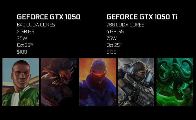
After a break of a couple of months in their Pascal launch schedule, NVIDIA is back again to launch a new Pascal desktop product. Following their near-perfect top-down launch schedule that started with GeForce GTX 1080 in May, being announced today and formally launching next week is the GeForce GTX 1050 Ti and GeForce GTX 1050. Aimed at the entry level discrete video card market, these products will round-out the GeForce 10-series desktop lineup.
Launching their low-tier cards last instead of first for the Pascal generation marks an interesting inverse of what happened with the Maxwell generation. In 2014 it was the low-end Maxwell 1 parts that launched first, only to be followed up by the other Maxwell 2 parts later on in the year. As a result, the Maxwell 2 family went through a full cycle – from release to retirement – before NVIDIA’s entry-level cards were refreshed. Out of all of the segments in the NVIDIA product stack, it’s fair to say that the entry-level was the one most due for a refresh.
And to that end, here we are with the GeForce GTX 1050 series. The previous GeForce GTX 750 series went very well for NVIDIA, so much so that the new 1050 series follows a number of beats laid out by its predecessor. NVIDIA is launching two cards – both of which are based on the new GP107 – which setup a two-tier product offering for the entry level market. The fast of the two cards is the GTX 1050 Ti, while the GTX 1050 follows closely to offer a bit less performance at a lower price point. And in order to maximize compatibility, both cards are being offered in configurations that draw their power entirely from the PCIe bus, forgoing the need for an external power connection.
| NVIDIA GPU Specification Comparison | |||||||
| GTX 1060 3GB | GTX 1050 Ti | GTX 1050 | GTX 750 Ti | GTX 750 | |||
| CUDA Cores | 1152 | 768 | 640 | 640 | 512 | ||
| Texture Units | 72 | 48 | 40 | 40 | 32 | ||
| ROPs | 48 | 32 | 32 | 16 | 16 | ||
| Core Clock | 1506MHz | 1290MHz | 1354MHz | 1020MHz | 1020MHz | ||
| Boost Clock | 1709MHz | 1392MHz | 1455MHz | 1085MHz | 1085MHz | ||
| Memory Clock | 8Gbps GDDR5 | 7Gbps GDDR5 | 7Gbps GDDR5 | 5.4Gbps GDDR5 | 5Gbps GDDR5 | ||
| Memory Bus Width | 192-bit | 128-bit | 128-bit | 128-bit | 128-bit | ||
| VRAM | 3GB | 4GB | 2GB | 2GB | 1GB | ||
| FP64 | 1/32 | 1/32 | 1/32 | 1/32 | 1/32 | ||
| TDP | 120W | 75W | 75W | 60W | 55W | ||
| GPU | GP106 | GP107 | GP107 | GM107 | GM107 | ||
| Transistor Count | 4.4B | 3.3B | 3.3B | 1.87B | 1.87B | ||
| Manufacturing Process | TSMC 16nm | Samsung 14nm | Samsung 14nm | TSMC 28nm | TSMC 28nm | ||
| Launch Date | 08/18/2016 | 10/25/2016 | 10/25/2016 | 02/18/2014 | 02/18/2014 | ||
| Launch Price | $199 | $139 | $109 | $149 | $119 | ||
Diving into the specs, we’ll start with the GTX 1050 Ti. Based on a fully enabled GP107 GPU, this card is arguably the backbone of NVIDIA’s entry-level offerings. All-told, it has 6 SMs enabled – 60% that of GP106/GTX 1060 – so GP107 is a bit more than half of a GP106. The rest of the Pascal architecture has been scaled similarly; GP107/GTX 1050 Ti retains 2/3rds of the ROP and memory controller configuration, meaning we’re looking at 32 ROPs attached to a 128-bit memory bus. Notably, this is double the number of ROPs found on GTX 750, so all other factors held equal, GTX 1050 Ti will see a massive jump in ROP throughput compared to its predecessor.
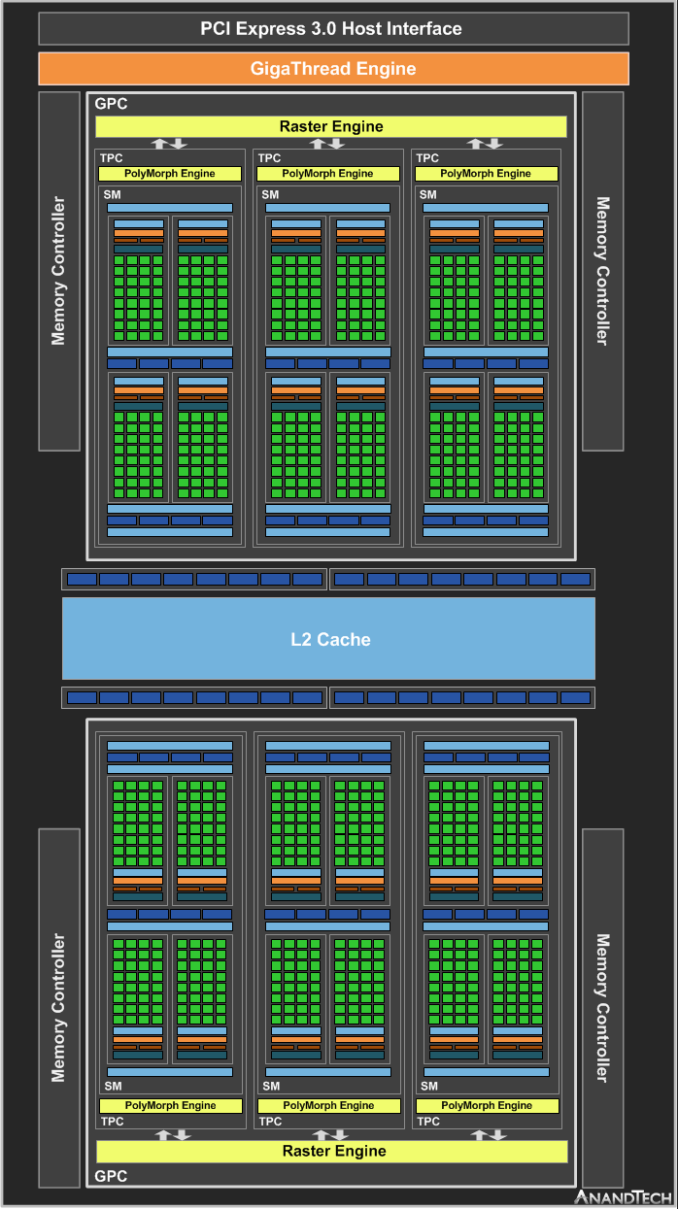
Unofficial GP107 Block Diagram
Feeding GTX 1050 Ti is 4GB of GDDR5 memory, clocked at 7Gbps. This is a budget card – and a power limited one at that – so NVIDIA has pulled back on the memory clocks compared to the other Pascal cards. Meanwhile power consumption starts at 75W, the maximum amount allowed to be pulled from a PCIe slot. I say “starts” because NVIDIA will be allowing partners to sell factory overclocked cards, and these cards will feature a higher TDP and an external power connector in order to meet the card’s power needs. The significance of offering a 75W-and-under card cannot be overstated; there is a sizable market for end users who would like to upgrade an OEM system but don’t have an external power connector, and this is a role the preceding GTX 750 filled very well. Meanwhile HTPC users who were holding out for a 75W card will be equally pleased, as now Pascal’s suite of media features are on a lower power card.
Joining the GeForce GTX 1050 Ti is its smaller, cheaper sibling, the GTX 1050. Based on a cut-down GP107 GPU, GTX 1050 drops 1 SM and 2GB of memory. This leaves us with a 5 SM (640 CUDA core) card paired with 2GB of GDDR5 running at 7Gbps. Otherwise it has the full ROP complement and memory bus, so while GTX 1050 loses some shader and geometry throughput, in other areas it holds firm. In fact due to the unusual clockspeeds of these cards – more on this in a moment – the GTX 1050 is actually clocked higher than the GTX 1050 Ti. So the net performance difference on paper is less than the loss of the SM; the smaller card should offer around 87% of the GTX 1050 Ti’s performance. With that said, unlike the last generation you don’t save any power versus the Ti card when going by the official TDP, as the GTX 1050 is also a 75W card, which happens to be 20W more than the GTX 750. Consequently while it’s still a card that can run on just PCIe slot power, by NVIDIA’s own numbers we may be looking at a relatively sizable increase in power consumption relative to its predecessor.
GP107 – An Enigma of a GPU
Having covered the basic specifications, I want to spill a bit more ink talking about the GP107 GPU. Reading the specs table, the GTX 1050 series cards are very unusual compared to their more powerful siblings. To be sure they’re still Pascal cards, but certain elements we take for granted about the Pascal family don’t apply here. At the same time there are certain elements we take for granted about x50 series cards which also aren’t applicable here. GP107 is, at the moment, an enigma of a GPU.
I’ll address what’s likely the elephant in the room first, which is the manufacturing process. To date all Pascal GPUs have been fabbed over at TSMC on their 16nm FinFET process. GP107 is not one of those GPUs. Instead, it’s fabbed on a 14nm process – NVIDIA’s specification sheet doesn’t technically state whose process – but by simple elimination it’s a very safe bet that they’re making the chip over at Samsung. Feature size is a red herring here, and instead the significance of this deal is that NVIDIA has not used a fab other than TSMC for GPUs for a long time. In fact we’d have to go back to 2003 to find an NVIDIA GPU fabbed somewhere else, when NVIDIA tapped IBM to help fab the ill-fated NV3x series (GeForce FX).
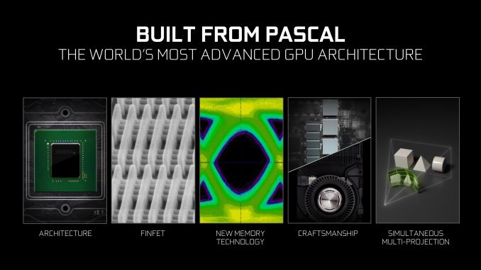
Suffice it to say, tapping another fab is a very big deal. There’s no second-sourcing here – GP107 is only being made on Samsung’s 14nm process and GP106+ only on TSMC’s 16nm process – but splitting orders like this may just as well be new territory for NVIDIA. As this is just a product announcement NVIDIA hasn’t said anything about the change in fabs, so let your imagination go wild here, but it definitely has some ramifications. I really need to get the GTX 1050 cards in house and on the testbed to figure out the full ramifications of this, but I think the most important change here is that a new process from a new vendor means that the voltage/frequency curve we’ve come to know with TSMC 16nm and Pascal has essentially been thrown out the window.
This in turn may explain the clockspeeds of the GTX 1050 cards. All of the other desktop GeForce 10-series cards have an official boost clock of 1600MHz+, with all but one of those cards being 1700Mhz+. The massive jump in clockspeed relative to Maxwell 2 is one of the signature elements of the Pascal architecture, and a major factor driving the significant performance gains of this generation compared to the last. The GTX 1050 series, by comparison, is only rated to boost up to 1455MHz for the GTX 1050, and lower still for the GTX 1050 Ti at 1392MHz.
Given that these are power-constrained cards, the final specifications of the cards are bound by a larger number of variables than usual – power curves, attainable frequency range, and now total power consumption – so I’m not even going to try to insinuate that the lower clockspeeds are solely a function of the change in fabs. However it’s very important to keep in mind that these lower clockspeeds come with a sometimes sizable increase in TDP relative to the GTX 750 series; instead of 55W/60W cards, we have 75W cards. So to use the fully enabled GTX 1050 Ti as an anchor point, power consumption has gone up 15W (25%) for a 28% increase in the boost clock, 1 more SM (20%), and somewhat decoupled from this, the doubled ROP count.
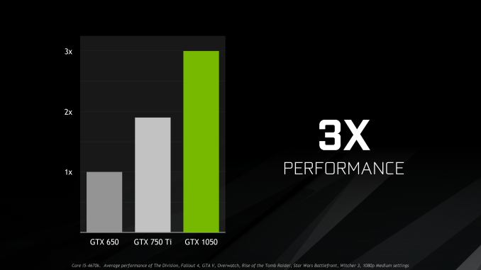
It’s telling then that NVIDIA has informed the press that the higher TDP cards with an external power connector are going to have much higher boost clocks. Whatever is going on under the hood, power plays a big part, and at a TDP limit of 75W, GP107 isn’t getting all the room it needs to stretch. Meanwhile it’s also noteworthy that NVIDIA’s own marketing materials call for GTX 1050 to have a 3x performance increase over GTX 650, and only a bit over 50% increase over GTX 750 Ti.
At the same time though, keep in mind we’re looking at a generation and a half architectural jump from the GTX 750 series (GM107) to the GTX 1050 series (GP107). So NVIDIA has to spend quite a bit of their transistor budget on supporting new features, and not just graphical features like SMP and Feature Level 12_1, but also features like the new video display block and the full fixed-function HEVC encode and decode blocks. By virtue of being the smallest Pascal, GP107 spends relatively more die size and space on non-graphics features. For those reasons the transistor count is quite a bit larger than GM107; NVIDIA has gone from 1.87B transistors to 3.3B, an increase of 76% (greater than the increase for any of the other Pascal GPUs). Or to put this another way, GP107 is 75% of the transistor count of GP106. Die size meanwhile stands at 135mm2, down a bit from the 148mm2 die size of GM107.
Ultimately GP107 is not just another Pascal GPU. While it offers the same feature set, there’s more than meets the eye, and it will be interesting to see how things shake out in benchmarking and overclocking. Ahead of launch, this is easily the least predictable GPU and card set of the entire Pascal family.
GTX 1050 Series Launch Info – No Reference Cards, GTX 1050 Ti Available Next Week
Getting back to the cards at hand, let’s talk about positioning, pricing, and availability. As these are NVIDIA’s entry-level cards, it goes without saying that they’re not targeted at NVIDIA’s usual horde of PC gaming enthusiasts. These cards won’t have the power to run games at 1080p with all the bells and whistles turned up – that’s really what the GTX 1060 is for – but instead they’re meant to be the next step up from integrated GPUs. This is a market that the GTX 750 series served very well (and judging from market share, NVIDIA sold well to), and the GTX 1050 will do the same. From specifications alone, the GTX 1050 series should be head and shoulders above the Intel GT2 iGPU found on Skylake/Kaby Lake.
Unlike the GTX 750 series, NVIDIA won’t be producing any reference cards this time around, Founders Edition or otherwise. So all GTX 1050 series cards are going to be vendor custom designs. Expect a mix of cards that follow the 75W TDP and cards that offer factory overclocks in exchange for a higher TDP. If for some reason you’re after a slot-powered card, be sure to check the specifications closely.
Meanwhile, although NVIDIA is listing the launch date as the 25th for both cards, from what NVIDIA has told me at the product briefing, in reality this isn’t quite the case. GTX 1050 Ti should in fact be available next week, right in time for the launch. However NVIDIA is not expecting GTX 1050 to be in stock for a few more weeks. Vendors can sell the cards as soon as they have them, so indeed the retail embargo ends on the 25th, but if the GTX 1050 interests you, don’t expect to be able to buy it until around mid-November.
Finally, let’s take a look at the completive landscape. Besides the outgoing Maxwell 1 and Maxwell 2 cards, the current-generation competition for the GTX 1050 series is AMD’s already-launched Radeon RX 460. The $109 GTX 1050 is the very clear counterpart to the 2GB RX 460. Meanwhile the $139 GTX 1050 Ti is in a bit of a different place; the cheaper 4GB RX 460 cards are running closer to $120 right now, so the GTX 1050 Ti is essentially $20 more expensive, which is a small but still significant difference given the overall low prices of entry-level cards. Still, it means that AMD’s two-month run as the sole supplier of current-generation entry-level video cards is about to come to an end.
| Fall 2016 GPU Pricing Comparison | |||||
| AMD | Price | NVIDIA | |||
| Radeon RX 480 (8GB) | $249 | GeForce GTX 1060 6GB | |||
| Radeon RX 480 (4GB) | $229 | ||||
| Radeon RX 470 | $199 | GeForce GTX 1060 3GB | |||
| $139 | GeForce GTX 1050 Ti | ||||
| Radeon RX 460 (4GB) | $119 | ||||
| Radeon RX 460 (2GB) | $109 | GeForce GTX 1050 | |||


↧
The Samsung 960 Pro (2TB) SSD Review
A year ago, Samsung brought their PCIe SSD technology to the retail market in the form of the Samsung 950 Pro, an NVMe M.2 SSD with Samsung's 3D V-NAND flash memory. The 950 Pro didn't appear out of nowhere—Samsung had shipped two generations of M.2 PCIe SSDs to OEMs, but before the 950 Pro they hadn't targeted consumers directly.
Now, the successor to the 950 Pro is about to hit the market. The Samsung 960 Pro is from one perspective just a generational refresh of the 950 Pro: the 32-layer V-NAND is replaced with 48-layer V-NAND that has twice the capacity per die, and the UBX SSD controller is replaced by its Polaris successor that debuted earlier this year in the SM961 and PM961 OEM SSDs. However...
↧
Huawei announces the HiSilicon Kirin 960: 4xA73 + 4xA53, G71MP8, CDMA
%20Main_575px.jpg)
Last year we had the opportunity to attend HiSilicon's launch event of the Kirin 950. The 950 SoC was the first to employ ARM's Cortex A72 in a smartphone, and the big.LITTLE 4x4 A72/A53 configuration of the 950 powered most of Huawei's flagships for 2016. It also marked a significant jump both in performance as well as efficiency compared to previous Kirin chipsets. The CPU part especially made such a good impression in our review of the Mate 8, and at the time we estimated that it would easily trade blows with Qualcomm and Samsung's own custom ARM microarchitecture designs, Kryo and Exynos M1, in their respective SoCs and flagship smartphones. Ultimately the Kirin 950 exceeded our expectations, in part due to the rather lackluster showing of this year's custom-CPU powered Android devices.
The Kirin 950 was initially launched in the Huawei Mate 8, their new flagship smartphone. The SoC then followed into the Huawei P9, P9 Max, and the Honor 8 over the course of 2016 - essentially all the premium devices for Huawei and Huawei's sub-brands, and contributing to the 106 million smartphone sales Huawei recorded in 2016 (30% of which were devices over $450). This is the success that Huawei wants to emulate with the Kirin 960.
Earlier this year, ARM announced their next generation microarchitecture IP in the form of the Cortex-A73 general-purpose core and the Mali-G71 graphics core. The A73 is a departure from the design of the A72 - the A72 was related to the A57 and A15 (Austin µarch family), whereas the A73 is a successor to the little-used Cortex A17 of the Sophia µarch family. Notable differences between the A73 to the A72 include a reduction of the decode-width from 3 to 2, but don't let this change fool you as the new micro-architecture is supposed to be both faster and smaller (and efficient) than that of the A72. On the GPU side, the Mali G71 is an even bigger upgrade for ARM as it marks the first IP of the Bifrost architecture which brings beyond a nomenclature change from the Mali-Txxx series also significant performance and efficiency improvements.
Back in May we said that we would expect SoCs and devices with these new IPs by the end of the year, and indeed, the new Kirin 960 SoC from Huawei's semiconductor subsidiary HiSilicon combines these two new technologies, promising the first commercial device to use them in due course.

While more details of the Kirin 960 will come forth over time as it makes its way into various devices, the official launch in Shanghai reiterated the partnership between HiSilicon and TSMC, using the new 16FFC process as the primary technology to enable the new SoC. As a reminder, the new process brings lower manufacturing cost thanks to lower mask count as well as better density due to new cell libraries.
| HiSilicon High-End Kirin Lineup | ||
| SoC | Kirin 950 | Kirin 960 |
| CPU | 4x Cortex A72 (2.3 GHz) 4x Cortex A53 (1.8 GHz) |
4x Cortex A73 (2.4 GHz) 4x Cortex A53 (1.8 GHz) |
| Memory Controller |
LPDDR3-933 or LPDDR4-1333 (hybrid controller) |
LPDDR4-1800 |
| GPU | ARM Mali-T880MP4 900 MHz |
ARM Mali-G71MP8 900 MHz |
| Interconnect | ARM CCI-400 | ARM CCI-550 |
| Encode/ Decode |
1080p H.264 Decode & Encode 2160p30 HEVC Decode |
2160p30 HEVC & H.264 Decode & Encode 2160p60 HEVC Decode |
| Camera/ISP | Dual 14bit ISP 940MP/s |
Improved Dual 14bit ISP |
| Sensor Hub | i5 | i6 |
| Storage | eMMC 5.0 | UFS 2.1 |
| Integrated Modem |
Balong Integrated UE Cat. 6 LTE |
Integrated UE Cat. 12 LTE 4x CA 4x4 MIMO |
The Kirin 960 features the same 4x4 big.LITTLE design implementation as the Kirin 950, but using four Cortex A73 cores at 2.4 GHz (by contrast, the Cortex A72 cores in the 950 were at 2.3GHz, and 2.5 GHz in the Kirin 955). The little cores remain of the Cortex A53 micro-architecture and at the same 1.8 GHz configuration.


Performance for the Kirin 960, as presented in Huawei's announcement, is +10% single core performance and +18% on the multi-CPU performance compared to the Kirin 950. (This isn't quite as much as we would have hoped from an A73 design, though.) HiSilicon presented GeekBench 4 scores for the new chipset and the K960 seems to benchmark around 2000 for single-core and 6400 for multi-core. The single-core scores slightly beat other Android SoCs in the market, however isn't a too drastic improvement. We don't have more exact sub-scores yet but one we know about is the vastly improved memory bandwidth of the new design that seems to beat all other SoCs at the moment. This is surely a result of both the Cortex A73's strong memory subsystem as well as new use of the CCI-550 in the Kirin 950 that also promised an increase in effective memory bandwidth over the preceding CCI-400 design.
Initially we expected A73 designs to use the improved power envelope to drive up the clock frequencies higher, however in the case of the Kirin 960 the A73 is merely 100MHz above the Kirin 950 and actually 100MHz slower than the 955's A72. The Kirin 950 already had the best sustainable CPU power envelope among this year's SoCs so it would be surprising if HiSilicon decided to limit performance lower power even more, however we have confirmation that that is exactly what happened as we've been told the CPU's power envelope has been lowered in favour of the GPU. This matches ARM's philisophy about the new A73 that was presented back at TechDay, so the Kirin 960 seems to put this philosophy into practice. While there wasn't talk about power efficiency we expect it to improve given that performance has gone up while power is supposed to have gone down.
Gallery: Kirin 960 Launch Presentation%20Main_thumb.jpg)
%20User%20Feedback_thumb.jpg)
%20Startup%20Time_thumb.jpg)
%20GB4%20CPU_thumb.jpg)
%20GB4%20DRAM_thumb.jpg)
%20andro4%20Storage_thumb.jpg)
A Bigger, Faster, More Powerful GPU
As mentioned earlier, the GPU sees a significant shift as we move from a Mali T880MP4 to a Mali-G71MP8, which essentially doubles the number of shader cores employed. HiSilicon decision to go with a wider GPU on the same process node was undoubtedly made much easier by the new G71's much better die area efficiency. The new GPU runs at 900 MHz, the same as the older SoC. The combination of doubling the shader cores over the 950 and moving to a new architecture over the 950 results in a 180% increase in the GPU's performance compared to the Kirin 950. As a result, Huawei is positioning the Kirin 960 directly above the other high-end SoCs launched this year (though we expect the other SoC vendors to also have respective increases with new generations soon). GFXBench Manhattan 3.0 and T-Rex Offscreen scores were showing the performance of the G71MP8 in above both the Snapdragon 820 and the Exynos 8890, but a tad under the new A10.

One of the popular criticisms of previous Huawei SoCs is the lack of graphics horsepower, with designs often opting for a four-core 'MP4' configuration despite using the high-performance graphics cores available from ARM. An MP4 configuration kept the die size of the SoC small and easier to implement. The downside of this is typically efficiency, suggesting that high graphics loads with fewer cores run at a worse point of the power efficiency curve to get an acceptable result.
Arguably most graphics scenarios on a smartphone, apart from extreme gaming titles and VR, can easily be provided by an MP4 configuration, and that was HiSilicon's main rationale for past GPU configurations. However as Huawei devices mature and get more premium, there is also the fact that when buying a device above $450, the user should expect something performing near the best in the market, and it was clear that an MP4 design could not do that. The fact that the Kirin 960 moves to an MP8 design, while increasing die area and maximum power consumption, means that a Kirin SoC moves up to compete with larger GPU configurations such as Samsung's large Mali designs in Exynos SoCs, Qualcomm's Adreno in the Snapdragons, or the 6-cluster PowerVR GPU in Apple's A-series. The mention of higher maximum power consumption comes with rather mixed feelings as the reasonably low GPU power was one of the aspects of the Kirin 950 that we especially praised when compared to other SoC designs, so we'll have to wait to see real devices to see if this improvement isn't a double-edged sword that introduces more severe GPU thermal throttling to the Kirin lineup.
Nevertheless, the improvement paves the way for things like VR, especially given Google's recent announcement of Daydream VR (starting with the Snapdragon 821 in the Google Pixel smartphone). With the right software support and display, we would expect all future devices using the Kirin 960 to support Daydream VR. With API support, the Kirin 960 will be promoted with Vulkan.
New Category 12/13 Modem with a Custom CDMA Implementation
The Kirin 960 also features a new HiSilicon based modem, allowing up to LTE UE Category 12/13 connectivity for up to 600 Mbps transfers, equaling the specifications of Qualcomm's Snapdragon 820 or Samsung's Exynos 8890 modems. The modem is being promoted as the first commercial SoC to provide quad carrier aggregation to meet that speed, although it will obviously require carrier support in the region in order to do so. The modem supports 4x4 MIMO (at only 2xCA) as well as up to 256QAM spatial stream modulation.

One of the more interesting announcements from the Kirin briefing was the implementation of CDMA in the modem. Currently three smartphone modem providers have CDMA solutions (Qualcomm in integrated and discrete modems, Intel with discrete, Mediatek with VIA-based integrated), and we spoke with HiSilicon to confirm that this is a brand new custom CDMA solution, rather than a licensed platform. The value of CDMA is mixed, although a required element with certain carriers in China and the US, such that Huawei can now offer devices with the Kirin 960 can compete. It should be pointed out that CDMA certification for the US via the FCC takes 18-24 months, and I was unable to confirm when the process was started, so we may have to wait another year for a US-focused CDMA devices.
We noticed that previous Kirin modem designs were made under the 'Balong' name, however the name is dropped for this model. We were told that Balong is an old brand, and it was being dropped at this performance level, although it is unclear if the modem in the Kirin 960 or future SoCs will be branded. This may be related to the fact that when asked about the presence of CEVA LTE IP in the modem similar to previous models, we were told that the LTE design in the new modem is a custom internal design without CEVA.

The multimedia capabilities of the new SoC have also seen a great improvement as we finally see 4K recording made possible. The new chipset supports 4K30 HEVC/H.265 decoding and encoding. The camera ISP is improved as well and brings new features natively supporting dual-sensor RGB/Monochrome configurations such as found on the Huawei P9 and Honor 8. Previously these had relied on an additional external ISP chipset to make use of the new monochrome sensor.
A Good Showing
Naturally we expect Huawei's next generation flagships to implement the Kirin 960 and variants over the next few months, especially as we move more towards Mobile World Congress in February. Similarly, updates to Kirin such as clock speed increases (the 955 is +200 MHz over the 950) moving into the middle of next year, along with an Honor device or two as time goes on. Huawei still keeps its HiSilicon SoC portfolio purely in-house, such that other smartphone OEMs do not have access to it, and given Huawei's current success in unit sales and revenue, we would expect the continue the status quo on this front.
As perhaps was to be expected, when we asked Huawei about competitor's 10nm plans (especially in light of recent news), no official statement was made. It's very hard to not try to theorise comparisons between the Kirin 960 and next year's Exynos and Snapdragons, while the former does bring substantial improvements to the table, it'll be a hard fight competing against the new generation. Given Huawei and HiSilicon's semiconductor product cycles, we might expect to hear more when TSMC's foundry business starts making more public noise about the availability of future nodes and silicon mass production (or even Intel, depending on relationships). We will probably have to tune in next year, perhaps at a similar time, and there may be more concrete news about chipset roadmaps.
We expect the first devices to use the Kirin 960 to come out shortly.
Further Reading
Andrei's Analysis of the ARM Cortex-A73 'Artemis' CPU Microarchitecture
Ryan's Analysis of the ARM Mali-G71 'Bifrost' GPU Architecture
The Huawei Mate 8 Review
The Honor 8 / Huawei P9 Review
↧
↧
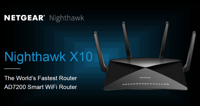
Netgear Launches 802.11ad-Enabled Nighthawk X10 (R9000) Wi-Fi Router
The Wi-Fi router market has seen a yearly cadence of flagship releases since the first 802.11ac routers came into the market in early 2012. Starting with 3x3 solutions, the market moved on to 4x4 and MU-MIMO-enabled Wave 2 solutions. We also saw Broadcom taking the lead with a dual 5 GHz radio solution (that has now been adopted by Qualcomm Atheros also). Many networking equipment vendors introduced solutions based on this. The recent mesh networking craze is also an offshoot of this dual radio solution - a dedicated 'invisible' channel is used to link the satellite to the main router (a discussion for another day). At CES earlier this year, the TP-Link Talon announcement indicated that tri-band Wi-Fi was getting traction in the market. Tri-band Wi-Fi involves radios operating in 2.4 GHz (802.11n), 5 GHz (802.11ac) and 60 GHz (802.11ad) bands. Today, Netgear is launching their first tri-band Wi-Fi solution - the flagship Nighthawk X10. It will be marketed as an AD7200-class router and will carry the R9000 model number.
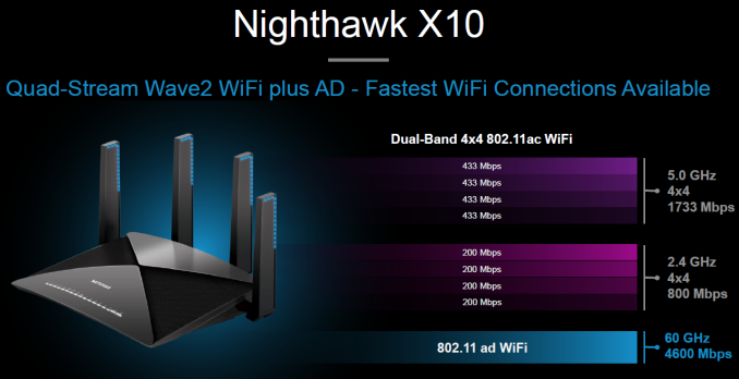
Similar to the other AD7200 routers in the market, the Nighthawk X10 adopts a dual band 4x4 802.11ac solution for (1733 Mbps + 800 Mbps) and a 1x1 802.11ad solution for 4600 Mbps to justify the AD7200 tag.
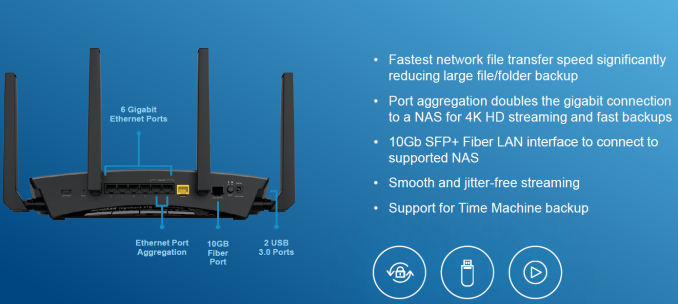
There are currently two 802.11ad routers in the market, the Acelink BR-6774AD and the TP-LINK AD7200 (Talon). Both models are pure Qualcomm solutions (i.e, the radios, switches and network processor are all from Qualcomm). The Nighthawk X10 aims to differentiate itself from the existing solution by integrating first-to-market features - both in terms of hardware and software. It is the first consumer router to sport a 10G network interface, and it is the first router capable of running Plex with transcoding capabilities in a standalone manner.
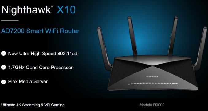
Qualcomm's IPQ solutions are pure network processors and do not have a video processing engine to enable the Plex capabilities that Netgear wanted to integrate in the Nighthawk X10. Therefore, Netgear decided to go with Qualcomm only for the radios (and, likely, the switches too). The network processing as well as the media capabilities are handled by a quad-core Annapurna Labs SoC running at 1.7 GHz. While Netgear didn't officially confirm the SoC model number, the specifications point to the Annapurna Labs AL-514 as the likely candidate. If this SoC sounds familiar to readers, it is the same as the one we saw in the Synology DS2015xs. It has four Cortex-A15 cores running at 1.7 GHz and comes with multiple network interfaces (including native 10G capabilities). Netgear claims that the AL-514 is the fastest router processor available for the consumer market. The exact layout of the board (number of switches and the way the link aggregation-capable network interfaces are hooked up to the SoC) will be interesting to analyze once the R9000 is out in the open market.
Netgear introduced their active antenna design (moving the TX power amplifiers from the board onto the detachable antennas) in the Nighthawk X8. In the X10, the RX power amplifiers are also moved out of the main board, further reducing noise concerns and improving robustness.
In addition to the obvious bandwidth advantages, 802.11ad also brings about a significant reduction in latency compared to 802.11ac. The 60 GHz band is not subject to interference like the 2.4 GHz and even the 5 GHz band now. These aspects makes the technology ideal for a number of use-cases that were simply not a good fit for traditional Wi-Fi. VR gaming and 4K streaming are being promoted by Netgear as ideal applications for the Nighthawk X10.
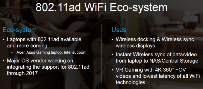
Unlike 802.11ac, where USB WLAN adapters were available for purchase when the first routers came into the market, the 802.11ad ecosystem is just getting started. There is an existing install base in terms of dedicated docking solutions, and Intel's newer vPro-enabled platforms have Wi-Gig support. However, it is not clear whether all existing Wi-Gig products in the market will be interoperable with the AD7200 routers. It must also be remembered that 802.11ad is a short-range line-of-sight technology - this means that the AD7200 routers can't be tucked away out of sight in a closet. The industrial design of the R9000 is similar to previous routers, and I am not entirely sure the market appreciates that in the living room (often cited as the reason for the attractively designed mesh routers becoming popular). The other strange feature is the 10G SFP+ fiber port. My market research revealed no consumer NAS models with that network interface. A 10G BASE-T port would have been nice, but, that increases the BOM cost. Consumers must note that the real-world performance of 802.11ad, like all other Wi-Fi technologies, is nowhere near the theoretical numbers. Under ideal conditions, real-world TCP throughputs of the order of 1.7 Gbps can be expected.
Netgear is also aiming to simplify setup and operation of the unit with a new 'Netgear Up' router installation app for both iOS and Android. Various housekeeping tasks will also be supported in that app.
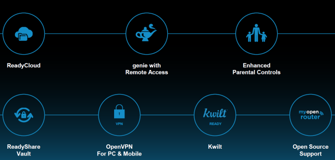
In addition, the usual set of Nighthawk features such as ReadyCloud, OpenVPN etc. are also supported. The R9000 will also be supported by the My Open Router Netgear open source community. However, installation of the open source firmware will result in loss of value-add features such as Plex.
The Netgear R9000 Nighthawk X10 is now available for purchase in retail as well as e-tail stores for $500.
↧
Acer Begins Selling 9.98-mm Swift 7 Kaby Lake Laptop in the U.S.: Starts at $1100
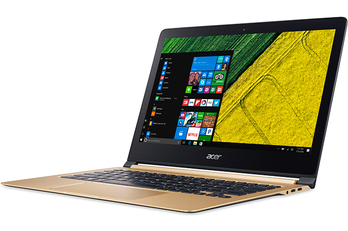
This week Acer has started to sell its first Swift 7 notebook in the U.S. The black and gold Swift 7 laptop is based on Intel’s Kaby Lake-Y-series CPU, and with an FHD display is the industry’s first clamshell PC that is thinner than one centimeter. The system is available now for $1099 from a number of retailers.
The Acer Swift 7 (SF713-51-M90J) comes in a black and gold aluminum unibody to emphasize that the device is one of the premium products in the manufacturer’s lineup. The thickness of the laptop with a 13.3” FHD display covered with Corning Gorilla Glass 4 is 9.98 mm (0.39”), which is thinner than Apple’s MacBook as well as Dell’s Adamo XPS, both of which are renowned for their thin form factors. As for mass, the device weighs 1.12 kilograms (2.48 lbs), which is a tad heavier than the MacBook.
Inside the Acer Swift 7 ultra-thin notebook there is an Intel Core i5-7Y54 processor (2C/4T, 1.2GHz/3.2GHz frequency, HD Graphics 615, 4.5 W), 8 GB of LPDDR3 RAM as well as a 256 GB SSD (the manufacturer does not specify whether it is an AHCI or NVMe). The laptop uses an 802.11ac Wi-Fi + BT 4.0 wireless adapter to communicate with the outside world wirelessly. The laptop also has a 720p webcam and two 5 Gbps USB 3.1 Type-C ports to connect peripherals, a display as well as for charging. Moving on to audio sub-system, we see a TRRS connector for headsets as well as two stereo speakers that are Dolby Audio certified.
| Acer Swift 7 | |||
| SF713-51-M90J | |||
| CPU | SKU | Core i5-7Y54 | |
| Base | 1.2 GHz | ||
| Turbo | 3.2 GHz | ||
| TDP | 4.5 W | ||
| GPU | SKU | Intel HD Graphics 615 (GT2) 24 EUs, Gen 9 |
|
| Base | 300 MHz | ||
| Turbo | 950 MHz | ||
| DRAM | 8 GB LPDDR3 | ||
| SSD | 256 GB | ||
| Display | 13.3-inch 1920x1080 IPS LCD | ||
| Ports | 2 x USB 3.1 (Gen 1) Type-C 3.5mm combo jack |
||
| Network | 2x2:2 802.11ac with BT 4.0 | ||
| Battery | 2770 mAh (52.9 Wh?) | ||
| Dimensions | H: 0.39" W: 12.78" D: 9.04" |
H: 9.98 mm W: 32.46 cm D: 22.96 cm |
|
| Weight | 2.48 lbs (1.12 kg) | ||
| Colors | Gold and Black | ||
| Price | $1099.99 | ||
Since the Swift 7 is powered by Intel’s Kaby Lake, expect significantly improved video encoding/decoding capabilities, better GPU performance, as well as Speed Shift v2 technology. This should make the new machine to be generally faster and snapper than ultra-thin notebooks based on previous-gen CPUs.
When it comes to battery life, Acer claims that the Swift 7 (SF713-51-M90J) has a 4-cell Li-Ion battery with 2770 mAh of capacity, which enables it to work for up to nine hours on one charge. Do note however that Acer does not specify conditions or workloads for that number.
The Acer Swift 7 (SF713-51-M90J) notebook is available directly from Acer as well as from leading retailers (Amazon, Newegg, etc.) for $1099.99. It comes with a one-year warranty. Finally, keep in mind that Acer plans to release a family of Swift 7 notebooks, as it revealed at IFA. So expect to see further models of the Swift 7, including a more affordable version based on Intel’s Core i3 at $1000, as well as a more advanced system featuring Intel’s Core i7-7Y75 and a higher price.


↧
Quantenna Announces 802.11ax Draft 1.0-Compliant Wi-Fi Chipset
![]()
Quantenna this week introduced the industry’s first 802.11ax Draft 1.0-compliant Wi-Fi chipset for access points. The QSR10G-AX is pin-to-pin compatible with Quantenna’s commercial QSR10G Wave 3 802.11ac-compliant Wi-Fi platform and can thus be easily integrated into existing APs (e.g., routers). The next-gen 802.11ax Wi-Fi standard promises to improve spectral efficiency of Wi-Fi operation in dense deployments and also to increase maximum theoretical bandwidth of Wi-Fi networks to around 10 Gbit/s.
Wi-Fi nowadays is a pervasive technology that is used by loads of different devices. Every office or residential building has tens of Wi-Fi APs visible and many people carry two or more of Wi-Fi-enabled devices with themselves (a smartphone, a laptop, most recently, smart watches). As a result, the number of connections that every AP needs to handle is getting higher every year, which requires higher spectral efficiency and more channels to connect devices. In the recent years the 802.11 standard introduced multiple ways to improve spectral efficiency of Wi-Fi, including multiple-input multiple-output antennas (MIMO), multi-user MIMO (MU-MIMO), higher order modulation and so on. The next-gen 802.11ax will add OFDMA (Orthogonal Frequency-Division Multiple Access) to allow different devices to be served by one channel, by dedicating different sub-carriers for individual client devices.
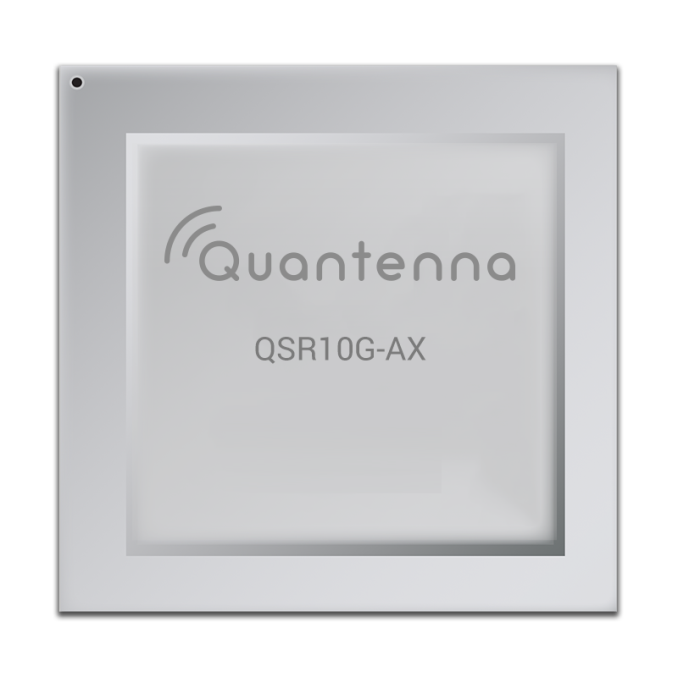
Quantenna’s QSR10G-AX is one of the industry's first 802.11ax Draft 1.0-compliant Wi-Fi chipsets, and supports the major features of the upcoming standard (including OFDMA, 1024-QAM and so on). Furthermore, to simplify deployment, it can be installed into existing designs due to pin-compatibility with the current QSR10G chipset. From a physical standpoint, devices based on the QSR10G-AX will use Quantenna’s 12-stream Wave 3 802.11ac dual-band Wi-Fi platform, which offers 8 streams in the 5 GHz band and a further 4 streams in the 2.4 GHz band. This essentially means that manufacturers using the QSR10G can simply throw in a more advanced chip and build an 802.11ax Draft 1.0-compliant router.
Right now, Quantenna does not specify the speeds that devices based on its QSR10G-AX will be able to provide, primarily because a lot will depend on actual client equipment. In the best case scenario with the currently available devices we are looking at 1733 and 2167 Mbps using four 802.11ac streams with 600, 800 and 1000 Mbps per stream. Nonetheless, keep in mind that the whole point of the 802.11ax is not to skyrocket maximum bandwidth (even though, maximum bandwidth remains important and does improve), but to ensure the ability to robustly serve the greatest number of clients using a single AP.
Meanwhile, the availability timeframe for such routers is unknown. Quantenna plans to make the QSR10G-AX chip available to its partners in early 2017. Then, it is going to take them some time to ensure that everything operates as planned (an uneasy thing to do due to lack of 802.11ax-compliant client equipment) and only then actual devices are set to hit the market.
↧
AnandTech Call for Writers: 2016
The Call for Writers has become something of an annual tradition over here at AnandTech. As anyone who follows the site knows very well, the list of things we have to review/cover usually exceeds our available time. So the call for writers gives us a chance to find new talent and new opportunities to grow, be it into new coverage areas entirely or just covering more of the existing products our readers have come to enjoy over the years.
The ultimate purpose of the Call for Writers is to find new talent. To continue to grow and improve our content, we need your help. We're looking for writers with a true passion for the technology we cover, a deep understanding of what's out there and a thirst for more knowledge.
We're looking for contributors to help out both with reviews as well as our short to medium form Pipeline coverage. The areas in particular we're looking for help with are listed below:
- News/Pipeline (US & Euro)
- Systems/Laptops (US-only)
- GPUs (US-only)
- Mobile/Smartphones
- Wearables
- Podcast Editor
- Networking
- Memory
- Monitors
- Home Automation/IoT
- Professional Graphics/GPU
If you find yourself at the intersection of knowledge and passion about any of those areas, and have some time to contribute, you're exactly what we're looking for. These are paid, part-time positions that we're looking to fill, with most positions open on a world-wide basis, and certain positions primed for a quick promotion to full-time. What I need is a writing sample that demonstrates your ability to talk about any one of these topics. Your sample can be in the form of a review, a pipeline post or an analysis piece - it should be something that looks like it would fit in on AnandTech.
Once you've produced it, send it on over to callforwriters@anandtech.com. Please also include a description of what subject(s) you would be interested in writing about, and some basic information about your background and where you're located. We'll read through all samples but can't guarantee a reply due to the sheer volume of submissions we tend to receive. If we like what you've sent and there's a potential fit on the team, we'll be in touch.
I'll conclude this post with a passage from our About page:
In the early days of technology reporting on the web the focus was almost exclusively on depth. We had a new medium for content that didn't come with the same restrictions as more traditional forms. We could present as much data as we felt was necessary and we could do it quicker.
As the web grew, so did the approach to gaining readership. In many cases, publishers learned from the tips and tricks of more traditional media to growing their audience. The focus shifted away from ultimate understanding of what was being reported, to producing content significantly motivated by increasing traffic, or revenue, or both. Thorough observations were out; sensationalism, link baiting, and the path to shallow 10-o'clock-news reporting were in.
While I believe it's definitely easier to produce content by going this route, I don't believe it's the only way to build a well read website.
If the above resonates with you and you'd like to help by being a part of something different, I'd encourage you to submit a writing sample.
Frequently Asked Questions
Q: How old do I need to be to work for AnandTech?
A: You need to be old enough to legally work in your country of residence without significant restriction. Otherwise we have no specific requirements so long as you can do the job well. Anand started the site at 14, after all...
Q: Do I need to be located in the United States to work for AnandTech?
A: Some positions do require that you be in the US for logistical reasons, and those specific positions are noted. However unless otherwise noted, most positions are open on a world-wide basis.
Q: Do I need to supply my own products for testing or contacts at companies? (i.e. do I need to be an insider?)
A: No. Assuming for the moment you have a computer to write on, then you already have the most important piece of equipment that you need. Meanwhile you will need some knowledge of the field at hand, but we will introduce you to the people you need to know for your position at AnandTech.
Q: Can I really work for AnandTech even though I don't have a Ph.D in electrical engineering?
A: Yes! We are first and foremost looking for people with a passion to learn, and the knack to make it happen. There's a certain degree of baseline knowledge needed for any given position, but if you can read existing AnandTech articles then you're already half-way there.
Q: Is there a submission deadline?
A: We have a tentative end point for the middle of November.
↧
↧
Chinese Tech Giant LeEco Enters US Market with Le Pro3 and Le S3 Smartphones, Range of UHD TVs
LeEco announced its official entry into the U.S. market at its “Ignite the Eco World” event in San Francisco, an important step in the company's globalization plan. Its initial products include two large-screen smartphones, a range of 4K TVs, and new content partnerships.
LeEco may be the biggest tech company you’ve never heard of. The Chinese company began life as LeTV in 2004 as a streaming content provider and is often referred to as the “Netflix of China.” It then began creating its own movie and TV content with its Le Vision Pictures studio and then expanded into hardware, selling TVs that plugged into its streaming service. More recently, it has expanded its hardware lineup to include smartphones and even a connected bicycle and electric car. It even has its own Uber-like taxi service in China, Yidao.
LeEco now looks to extend its reach further west. Earlier this year it purchased U.S.-based TV maker Vizio, the second largest brand in the U.S., for $2 billion, giving it a familiar name and a foothold in a market wary of Chinese brands. LeEco also purchased Dichotomy Creative Group in September, rebranding it Le Vision Entertainment. The new division is headquartered in Los Angeles and will be responsible for creating original English-language content spanning movies, TV, VR, and the Web. LeEco is even setting up its global headquarters in Silicon Valley (its campus in Beijing will remain its headquarters for China), having purchased a 48-acre plot of land in San Jose, California from Yahoo that will eventually employ some 12,000 people.
| LeEco's US Ecophone Lineup | ||
| Le Pro3 | Le S3 | |
| SoC | Qualcomm Snapdragon 821 (MSM8996 Pro) 2x Kryo @ 2.34GHz 2x Kryo @ 2.19GHz Adreno 530 @ 653MHz |
Qualcomm Snapdragon 652 (MSM8976) 4x Cortex-A72 @ 1.80GHz 4x Cortex-A53 @ 1.44GHz Adreno 510 |
| Display | 5.5-inch 1920x1080 IPS LCD | 5.5-inch 1920x1080 IPS LCD |
| Dimensions | 151.4 x 73.9 x 7.5 mm 177 grams |
151.1 x 74.2 x 7.5 mm 153 grams |
| RAM | 4GB LPDDR4 | 3GB LPDDR3-1866 |
| NAND | 64GB | 32GB (eMMC 5.1) |
| Battery | 4070 mAh non-replaceable Qualcomm Quick Charge 3.0 |
3000 mAh non-replaceable Qualcomm Quick Charge 3.0 |
| Front Camera | 8MP, 1.4µm pixels, f/2.2 | 8MP, 1.4µm pixels, f/2.2 |
| Rear Camera | 16MP, f/2.0, PDAF, dual-tone LED flash | 16MP, f/2.0, PDAF, HDR, dual-tone LED flash |
| Modem | Qualcomm X12 LTE (Integrated) 2G / 3G / 4G LTE (Category 12/13) |
Qualcomm X8 LTE (Integrated) 2G / 3G / 4G LTE (Category 7) |
| SIM Size | NanoSIM | 2x NanoSIM (dual standby) |
| Wireless | 802.11a/b/g/n/ac, BT 4.2, NFC, IrLED, GPS/GNSS | 802.11a/b/g/n/ac, BT 4.1, IrLED, GPS/GNSS |
| Connectivity | USB 2.0 Type-C | |
| Launch OS | Android 6.0.1 with EUI 5.8 | |
| Launch Price | $399 | $249 |
To kickstart its U.S. strategy, LeEco is offering two smartphones: the Le Pro3 and the Le S3. Both phones have 5.5-inch 1080p displays, but use different internal hardware. The Le Pro3 includes Qualcomm’s latest Snapdragon 821 SoC, 4GB of LPDDR4 RAM, and 64GB of internal storage. Given its emphasis on streaming content it’s probably not too surprising it does not offer additional storage tiers or microSD card support. Its most interesting feature is a large 4070mAh battery, which should help keep the screen lit for extended movie watching.
The Le S3 comes with a Qualcomm Snapdragon 652 SoC, which combines four ARM Cortex-A72 CPU cores, four Cortex-A53 cores, and an Adreno 510 GPU that supports all of the latest 3D graphics APIs. We saw its smaller sibling, the Snapdragon 650 that comes with two fewer A72 cores, push the performance of Xiaomi’s Redmi Note 3 Pro to near flagship levels, so the Le S3 has good performance potential; however, in my brief time with the phone, I noticed some stuttering when navigating the UI and far too many instances where frame rate dropped below 60fps, more so than with the Redmi Note 3 Pro.
The Le S3 also comes with 3GB of LPDDR3 RAM, which should be adequate, but only 32GB of internal storage. For a device that needs to cache lots of music and videos, and still have room for pictures and apps, we definitely would like to see more NAND, especially without microSD card support. The Le S3 also does not get a big battery like the Pro3; its 3000mAh cell is a typical size for 5.1- to 5.2-inch phones rather than a 5.5-inch phablet.

Le Pro3 (left), Le S3 (right)
Both phones have a similar camera setup, with an 8MP front-facing camera and a 16MP primary camera that has an f/2.0 lens and PDAF for faster focusing but does not include optical image stabilization (OIS). Video recording options are pretty basic, supporting only 2160p30 (4K), 1080p30, and 720p30 modes, and with no electronic image stabilization (EIS) option, videos can look pretty shaky.

Le S3 (rose gold)
LeEco eliminated the 3.5mm headphone jack from its phones before Apple axed the analog port in its iPhone 7, opting to pass audio over the USB Type-C port instead. Both the Le Pro3 and Le S3 support LeEco’s Continual Digital Lossless Audio (CDLA) technology that passes digital audio over USB. CDLA compatible earphones, included with both phones, have their own DAC and audio processor that’s supposed to reduce noise and improve channel separation relative to traditional analog audio from a 3.5mm jack. A Type-C to 3.5mm adapter is also included so you can use traditional headphones too.
Both phones also support Dolby Atmos surround-sound technology thanks to the Snapdragon SoCs, which produces more realistic positional audio and even accounts for an object’s vertical position in the soundfield as well.

The Le Pro3 and Le S3 both use aluminum unibody construction and share a similar design language. On the back of the phones we find horizontal plastic antenna lines at the top and bottom, with a large, not-quite-circular camera surround and fingerprint scanner. LeEco was the first company to use Qualcomm’s ultrasonic Sense ID fingerprint sensor, but these phones are using the more common capacitive variety. The most obvious visual difference between the phones is the finish applied to the aluminum: The Le Pro3 has a brushed finish while the Le S3 has a sandblasted finish.

The phones also look quite similar from the front, with relatively small upper and lower bezels and a symmetric layout. Hiding behind the lower bezel is a set of capacitive, backlit buttons. The LeEco logo replaces the standard home glyph on the Pro 3 and is flanked by the recents and back buttons of the left and right, respectively. The only other difference is that the Pro 3 uses 2.5D curved glass, while the S3’s edge-to-edge Corning Gorilla Glass 3 is flat all the way to the edge, giving it a sharper feeling in the hand.
One thing that’s immediately obvious as soon as you turn on either phone is the ridiculously large black bezel on all sides of the screen. The black area is significantly larger in person than LeEco’s press renderings show. I have not seen a border this large on a phone in some time, at least not on a phone that costs more than $200. For me, it’s large enough to be distracting and, in my opinion, it gives the phones a low-cost look.

Both phones include an infrared LED on the top edge for remote control duties, which fits in with LeEco’s philosophy of enabling its hardware to work together. Centered on the bottom edge is a USB 2.0 Type-C port flanked by two perforated grilles. On the Pro 3 they’re covering a pair of speakers, although, having both so close together and firing downward will diminish the stereo effect.
Switching our focus to software, we find that both phones are still running Android 6 Marshmallow with LeEco’s Ecosystem User Interface (EUI) 5.8 running on top. It’s disappointing that the phones will not ship with Android 7, but the demo models I handled were at least running recent security patches (either September or October). What’s unique about EUI are the included apps and built in support for accessing LeEco’s streaming content. Swiping to the left of the default home screen opens LeView, a list of suggestions for video content that learns from your viewing habits, somewhat analogous to HTC’s BlinkFeed or Flipboard for news. Tapping the Live icon opens a 3x3 grid of live video previews of content available for streaming. The Le app gives more comprehensive access to LeEco’s catalog of videos, TV episodes, and music.

It should be obvious by now that LeEco’s business strategy is more Amazon than Apple; it makes money from selling content and uses hardware as a delivery system. Because its revenue is not hardware-focused like with many of its competitors, it can sell its products at competitive prices, even at cost if necessary. LeEco’s ultimate goal is to create an internet-connected ecosystem encompassing hardware, software, and content that provides seamless access to all forms of digital entertainment. That’s no easy task, especially in the U.S. where many entrenched companies, including cable providers, movie studios, TV broadcasters, and internet companies provide similar services, albeit not always in a holistic way.
LeEco thinks it has the answer to this problem with its EcoPlatform that’s open to third-party content providers and hardware partners, essentially giving them access to LeEco’s content delivery system with its apps and LeCloud network that encompasses more than 750 CDN nodes. LeEco announced a number of launch partners at its event, including Lionsgate, Showtime, Esquire, the History Channel, and Metro-Goldwyn-Mayer to name just a few, and it mentioned that another major content partner will be announced on November 2.
To get the most from an ecosystem, whether it’s Apple’s or Google’s or Amazon’s, you need to fully buy in. This is especially true with LeEco, where signing up for Le EcoPass grants you access to 5TB of cloud storage, unlimited monthly movie viewing, extended warranties on LeEco hardware, and access to two EcoPass days (think Black Friday sales) at LeMall.com, its online storefront. It also offers the LeRewards program that grants further discounts on products.

Both the Le Pro3 and Le S3, along with LeEco’s other products, will be available for purchase on November 2 at LeMall.com. The Le Pro3 will cost $399 and the Le S3 will cost $249. There will be a $100 LeRewards discount available for both phones, which will drop the prices to $299 and $149, respectively. The Le Pro3 will be available in two colors—gray and gold—while the Le S3 will be available in three colors—gray, gold, and rose gold. Both phones will be unlocked and are compatible with GSM networks from AT&T, T-Mobile, MetroPCS, and Cricket Wireless.
↧
Razer Re-Launches The Razer Blade Pro: GTX 1080 And 4K G-SYNC
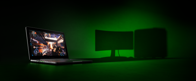
It’s been a while since Razer has refreshed the Razer Blade Pro, which is their 17.3-inch desktop replacement laptop. The outgoing model still has a Haswell processor with GTX 960M. It’s always been a bit strange that the 14-inch Razer Blade was equipped with a stronger GPU than the larger laptop, and when the Razer Blade Pro was last updated, the Razer Blade had a GTX 970M in a smaller form factor.
This is no longer the case. The 14-inch Razer Blade was just updated with Skylake and GTX 1060 in September, which should significantly increase its performance, and today Razer is announcing the new Razer Blade Pro, which finally surpasses its smaller sibling in performance with a NVIDIA GeForce GTX 1080 squeezed into the same 0.88-inch thick CNC aluminum chassis. The Core i7-6700HQ 45-Watt CPU replaces the outgoing Haswell processor, and 32 GB of DDR4 RAM is now available. In order to keep the system cool, Razer has designed what they are calling the world's thinnest maufactured vapor chamber cooling solution in a laptop. Combined with a custom fan design and a dynamic heat exchanger, Razer is engineering as much cooling as they can into the thin notebook.

Razer has been a big proponent of IGZO displays, and they have outfitted the Blade Pro with a 17.3-inch 3840x2160 IGZO IPS display, and this high-resolution panel also supports NVIDIA’s G-SYNC technology, which should help quite a bit with gaming, even with the big GPU under the hood. This display covers 100% of the Adobe RGB color gamut as well, just like the Razer Blade Stealth UHD model. That has implications though due to the lack of proper color management in Windows, and if it is like the Stealth, it won’t have any included color management software. It’s not Razer’s fault, and hopefully more devices with wide color gamut support will force Microsoft’s hand here.

Razer has also outfitted the new Pro with their new ultra-low profile mechanical switches, which feature actuation points which register at 65 grams, as well as reset points. There have been other laptops with mechanical switches, but they are generally the full-size switches which require much more travel. On a 0.88-inch thick laptop, there would be no way for this to work. Razer has also added the same per-key RGB Chroma branded lighting they have already added to both the Stealth and Blade models.
The TrackPad sits to the right of the keyboard, much like on the older model, but if you are gaming, a mouse is likely the best bet.
| Razer Blade Pro | |||||
| CPU | Intel Core i7-6700HQ Quad-Core with Hyperthreading 2.6-3.5 GHz, 6MB Cache, 45W TDP |
||||
| GPU | NVIDIA GTX 1080 2560 CUDA Cores 1566-1733 (Boost) MHz 8GB 256-bit GDDR5X |
||||
| Memory | 32 GB DDR4 2133MHz | ||||
| Display | 17.3" 3840 IGZO IPS 100% Adobe RGB G-SYNC Enabled with multi-touch |
||||
| Storage | 512GB / 1TB / 2TB SSD PCIe M.2 RAID 0 (2 drives) |
||||
| I/O | USB 3.1 Type-C with Thunderbolt 3 USB 3.0 Type-A x 3 RJ-45 Gigabit Ethernet Killer E2400 Headset jack 2.0MP Webcam SDXC HDMI 2.0 |
||||
| Dimensions | 424 x 281 x 22.5 mm 16.7 x 11 x 0.88 inches |
||||
| Weight | 3.54 kg / 7.8 lbs | ||||
| Battery | 99 Wh, 250 W AC Adapter | ||||
| Wireless | Killer Wireless-AC 1535 802.11ac 2x2:2 with Bluetooth 4.1 Killer DoubleShot Pro |
||||
| Price | $3699+ | ||||
At under eight pounds, the new Blade Pro is actually pretty light for a system of this size and performance. The new Razer Blade Pro exceeds the requirements for any of the current VR headsets, so it should be able to run VR pretty well.

All of these features do add to the cost though. Where as the new 14-inch Razer Blade starts at $1800, the new Razer Blade Pro starts at over double that price: $3700. Shipments start in November.
Gallery: Razer Blade Pro![]()
![]()
![]()
![]()
![]()
![]()


↧
Nintendo Announces Switch Portable Gaming Console - Powered by NVIDIA Tegra
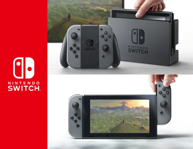
Earlier today Nintendo took the wraps off of their next generation console, Switch. Formerly known by the codename NX, the Switch is the successor to both Nintendo’s portable DS and set top Wii console lines, utilizing a portable, tablet-like unit that can be docked to behave like a set top console. Today’s announcement, in the form of a 3 minute trailer, is meant to tease the console ahead of its full launch in March of 2017.
While I’ll skip the commentary on the console’s unusual design – dedicated gaming sites can offer better context – I wanted to dive into the hardware in the Switch. Given that this was a teaser, I was not expecting a reveal of any of the hardware specifications of the console, and indeed neither Nintendo’s teaser video nor their related press release made any mention of the underlying hardware. However shortly after the reveal went live, NVIDIA sent out an email to the press and posted a blog of their own. As it turns out, while today is still just a teaser, in some ways we’re already getting more information about the console than in any previous generation of Nintendo’s hardware.
In their blog post, NVIDIA confirmed that they would be providing the underlying SoC for the console. As this is still ultimately a teaser, NVIDIA’s own details are light, but their announcement confirms that it’s a custom version of their Tegra SoC. Curiously, no mention of the CPU core in that SoC is mentioned. However as it’s a Tegra, something ARM-based is the logical (if not only) choice. And on the GPU side, as you’d expect, they’re using a GPU based on one of NVIDIA’s existing GPU architectures, though the company isn’t specifying if it’s Pascal or Maxwell (I’d assume Pascal, but consoles are known for their long development cycles).

Otherwise, as far as specifications go that’s all we get for now. Though as NVIDIA is supplying a whole SoC there are obviously many more parts to the package that we’ll hopefully learn about in the near future. More CPU and GPU details are obviously the most interesting aspect – does the Switch SoC use Denver CPU cores? – but there’s also the matter of memory bandwidth, WiFi support, and the many other functional blocks that make up an SoC.
For NVIDIA, this is the first console hardware win for the company since the PlayStation 3, which launched in 2006. In the set top console market, AMD has since provided the GPU (and often, the CPU) for the most recent generation of consoles. Otherwise NVIDIA has never had a 3rd party portable console win, primarily because both Nintendo and Sony developed their respective SoCs internally for the 3DS and Vita.
In fact, given that Nintendo previously did much of their portable console development work internally, this is a notable shift for how the company operates. The 3DS was essentially a custom SoC combining multiple ARM11 (ARMv6) CPU cores with an OpenGL ES 1.1 generation GPU from the little-known Digital Media Professionals (DMP). So this is the first time Nintendo has contracted out their SoC needs to a third party in such a visible fashion. I’m actually a bit surprised that NVIDIA is even allowed to talk about their involvement at this point in time, given Nintendo’s historical focus on secrecy.
Though all of this also helps to underline just how big a jump in technology the Switch is from the 3DS. On the CPU side alone it’s reasonable to assume we’re looking at CPU design in the neighborhood of 4.x DMIPS/MHz, versus ARM11’s approximate 1.3 DIMPS/MHz rate, so IPC will have increased significantly, never mind an increase in frequency. Meanwhile on the GPU side, Nintendo is going from a GPU that didn’t even have a programmable GPU pipeline (i.e. shaders) to a fully modern GPU, essentially catching up on a decade of mobile GPU development in a single bound. Given that the console has to work as both the company’s portable and set top consoles, Nintendo has opted to use far more modern tech than their traditionally conservative designs.

Finally, without reading too much into a 5 paragraph announcement, there is one other interesting nugget of information in NVIDIA’s blog post that further shows just how deep the NVIDIA/Nintendo relationship is going here. Along with providing the SoC, NVIDIA also has a major stake in the development of the console’s API and middleware. While NVIDIA presumably isn’t developing the entire software stack, they make special note of the fact that they are providing a new “lightweight” API, NVN, for the console. NVIDIA is also providing middleware in the form of “a revamped physics engine, new libraries, advanced game tools and libraries” and “custom software for audio effects and rendering” which sounds a great deal like NVIDIA having brought over major parts of their GameWorks SDK, including the PhysX physics simulation libraries and VRWorks Audio library.
In any case, it will be interesting to see how this plays out over the next few months. The mobile world has changed significantly since the 3DS was launched in 2011, something that the Switch’s design makes obvious. Nintendo has gone in a very different direction than either their console rivals or the smartphone market that is always threatening to encroach on mobile consoles, and that’s reflected in both the unusual dual-mode console and the hardware inside of it.
↧
Kodak Ektra Smartphone Announced: MediaTek Helio X20, 21 MP Camera, USB-C
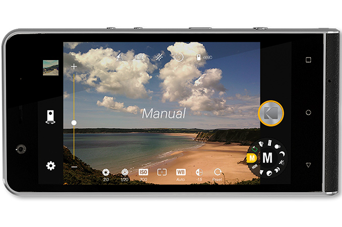
Eastman Kodak and the Bullitt Group on Thursday introduced the Ektra smartphone, which will be the first mainstream handset carrying the Kodak brand. The phone inherits its Ektra name from Kodak’s consumer cameras from the 1940s, and is designed to cater to digital photography enthusiasts, which is emphasized by overall design (which somewhat resembles the original), a large assembly of lenses as well as a dedicated shutter button. Initially, the Kodak Ektra device will be exclusively in Europe for €499.
Kodak developed the world’s first digital camera in the mid-1970s and has patented a huge number of digital imaging-related technologies since then. Although the company was fairly successful with its digital cameras in the 1990s and early 2000s, it lost a significant chunk of its market share later on as new companies entered the scene. Consequently, Kodak filed for Chapter 11 bankruptcy protection in early 2012 and then had to exit the digital camera business, sell off its image sensor solution unit and some other businesses, and then sell many of its patents to a group of high-tech rivals in 2013. After re-emerging from bankruptcy, Kodak decided to focus on commercial products and services, but did not forget its heritage of serving consumers. In 2013, it demonstrated its first micro four thirds camera to be made by a third party and in late 2014 announced plans for smartphones.
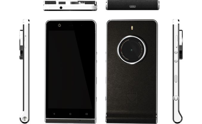
Nowadays the market for standalone cameras is on the decline as many people use smartphones to make pictures, and this is when Kodak decided to team up with Bullitt (which also has rights to produce phones under CAT and Land Rover brands) to create a Kodak-branded handset. Under the terms of the agreement, Kodak licensed two of its trademarks to Bullitt and then developed the photography software as well as the optical lenses assembly. In the meantime, Bullitt designed the Kodak Ektra smartphone itself.

From hardware point of view, the Kodak Ektra is a typical mainstream smartphone, featuring a 5” FHD display and is based on MediaTek’s Helio X20 SoC. The handset comes equipped with 3 GB of LPDDR3 RAM, 32 GB of NAND flash storage, a 802.11ac Wi-Fi + BT 4.1 wireless module, a 4G/LTE Cat4 modem and a 3000 mAh battery. A good thing is that the phone sports a USB Type-C port used both for data and charging.
| Specifications of Kodak Ektra | |||
| Kodak Ektra | |||
| SoC | MediaTek Helio X20 (MT6797) 2 × Cortex-A72 at 2.3 GHz 4 × Cortex-A53 at 2.0 GHz 4 × Cortex-A53 at 1.4 GHz ARM Mali T880 MP4 GPU at 780 MHz |
||
| RAM | 3 GB LPDDR3 | ||
| Storage | 32 GB + up to 128 GB microSD | ||
| Display | 5" 1920 × 1080 with Corning Gorilla Glass | ||
| Network | GSM/GPRS/EDGE: 850/900/1800/1900; WCDMA: 850/900/1900/2100; HSPA; LTE: 1/3/7/20 (Cat 4); |
||
| Dimensions | 147.8 × 73.35 × 9.69 mm 14.02 at camera lens |
||
| Weight | 163.8 grams | ||
| Rear Camera | Sony Exmor RS 21 MP sensor with F2.0, PDAF, OIS and dual-LED flash. The lense is covered with Corning Gorilla Glass. | ||
| Front Camera | 13 MP with F2.2 PDAF | ||
| Battery | 3000 mAh (5V, 2A charger) | ||
| Sensors | Ambient Light, Accelerometer, Gyroscope, Proximity sensor | ||
| OS | Google Android 6.0 Marsmallow | ||
| Software | Kodak Camera software Snapseed app for photo editing Super 8 app for video Prints app MobiSystems OfficeSuite AVG AntiVirus FileCommander |
||
| Connectivity | 802.11 ac Wi-Fi, Bluetooth 4.1, USB-C, 3.5mm for audio, FM Radio | ||
| Navigation | GPS + GLONASS | ||
| SIM Size | Nano SIM | ||
| Colors | Black | ||
| Launch Countries | E.U. | ||
| Price | €499, £449 | ||
Gallery: Kodak Ektra Smartphone![]()
![]()
![]()
![]()
![]()
![]()


Meanwhile, the imaging capabilities of the Kodak Ektra deserve a closer look: after all, the smartphone is all about photography. The main (rear) camera of the phone uses Sony’s 21 MP Exmor RS IMX230/IMX338 sensor (Kodak does not reveal the exact model), which is found on some other smartphones nowadays, as well as a dual-LED flash. As noted above, Kodak designed the imaging software with SLR-like UI to select the scene type (e.g., HDR, landscape, portrait, macro, sport, night-time, panorama, bokeh as well as a smart auto mode). In addition, the phone supports the manual mode that allows adjusting exposure, ISO, focus, white balance and shutter speed — just like on cameras. Finally, Kodak applied a special coating to the lenses to maximize their luminous transmission.
While Sony’s 21 MP sensors are used relatively widely and behave predictably, Kodak’s lens assembly and custom software are supposed to be the main factors that will differentiate the Ektra from competing Android 6-based devices. Obviously, we will need to test the hardware and software before drawing any conclusions about imaging capabilities of the Kodak smartphone. As for the front-facing camera, Bullitt/Kodak installed a fairly good 13 MP sensor with an f/2.2 lens.


Kodak and Bullitt intend to sell the Ektra in Europe later this year for €499 or £449, depending on the country, through Bullitt’s typical sales channels. The design as well as the price point clearly indicate that the Kodak Ektra is a niche phone that is positioned below flagship models from Apple and Samsung, but still relatively high in the market for what's largely mainstream hardware. That said, it looks like the Ektra is banking on people familiar with the Kodak brand, who value imaging capabilities, stylish design and original accessories (Kodak will offer a case and a pouch). However, it is unlikely that the smartphone will capture a significant chunk of the market. After all, many smartphone makers claim that their products have the industry’s best photography capabilities and Kodak/Bullitt are definitely not the first to advertise such features.


↧
↧
Intel Announces Q3 FY 2016 Earnings: Record Quarterly Revenue
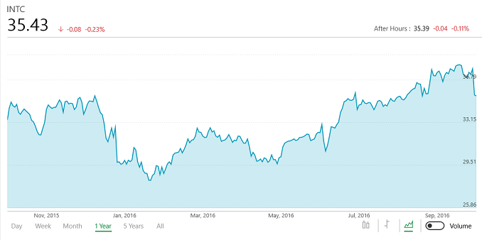
Earlier this week, Intel announced their earnings for the third quarter of their 2016 fiscal year, and the company achieved new records across their business lines, resulting in a record quarterly revenue of $15.8 billion USD, up 9% compared to Q3 2015. Intel achieved margins of 63.3%, up 0.3% year-over-year, and their operating income increased 6% to $4.5 billion. Net income for the quarter was $3.4 billion, up 9%, and earnings per share came in at $0.69.
| Intel Q3 2016 Financial Results (GAAP) | |||||
| Q3'2016 | Q2'2016 | Q3'2015 | |||
| Revenue | $15.8B | $13.5B | $14.5B | ||
| Operating Income | $4.5B | $1.3B | $4.2B | ||
| Net Income | $3.4B | $1.3B | $3.1B | ||
| Gross Margin | 63.3% | 58.9% | 63.0% | ||
| Client Computing Group Revenue | $8.9B | +18.7% | +5.7% | ||
| Data Center Group Revenue | $4.5B | +12.5% | +9.9% | ||
| Internet of Things Revenue | $689M | +20.4% | +18.6% | ||
| Non-Volatile Memory Solutions Group | $649M | +17.1% | -0.9% | ||
| Intel Security Group | $537M | flat | +6.1% | ||
| Programmable Solutions Group | $465M | -8.6% | - | ||
| All Other Revenue | $44M | +10% | -42.8% | ||
Intel also announced Non-GAAP results, which exclude certain things like acquisition-related adjustments, deferred revenue write-down, restructuring, and more. For a full list, please check out their lengthy explanation on their earnings report. On a Non-GAAP basis, revenue was the same $15.8 billion, margins were up 1.3% to 64.8%, and operating income was up 18% to $5.1 billion. Net income was up 21% to $3.9 billion, and earnings per share were up 21% to $0.80.
Intel’s internal divisions are broken down into six groups. The Client Computing Group, which is PCs, tablets, phones, and wired and wireless communication. The Data Center Group focuses on enterprise and the cloud. Internet of Things is retail, transportation, industrial, building, and home use electronics. Non-Volatile Memory Solutions is mostly Intel’s SSD efforts. Intel Security Group is security software (McAfee) and new for fiscal 2016 is the Programmable Solutions Group, formed after the acquisition of Altera, and features field-programmable gate arrays and related products.

For Q3, the Client Computing Group had revenues of $8.892 billion, which is up from $8.506 billion a year ago. Unit volumes were actually down 4% compared to the same point a year ago, and volumes are down 11% for the year compared to the first three quarters of 2015, but average selling prices (ASP) continue to increase. For this quarter ASP was up 6% compared to a year ago, and is up 12% for the year so far. Breaking it down a bit further, Intel has had 4% growth in notebook platform sales for this quarter (year-over-year) with ASP up 3% in the notebook segment. Desktops dropped 6% in volume, but have kept the same average selling price, and “tablet platform volumes decreased” which is a non-numerical way to say that Intel is getting out of the dedicated tablet market altogether.
The Data Center Group had revenues of $4.542 billion this quarter, up from $4.140 billion a year ago. Unit volumes increased 12% this quarter compared to Q3 2015, and for the year unit volumes are up 9%. Average selling price has decreased though, down 3% this quarter, and down 2% for the year so far.
Intel doesn’t break out the numbers as specifically for the remaining groups, but Non-Volatile Memory Solutions had revenue that was more or less flat at $649 million for the quarter, compared to $655 million a year ago. Internet of Things continues to grow, up to $689 million in revenue, compared to $581 million in Q3 2015. The Intel Security Group increased revenue from $506 million to $537 million, and the Programmable Solutions Group had revenue of $425 million, with no comparison to last year since it is a newly acquired product group, but up 6% compared to Altera’s numbers from last year.
Intel has made some announcements in this quarter as well. Intel started sampling Stratix 10 in this quarter, which is the only 14 nm FPGA. They also announced they will sell 51% of the Intel Security Group, and establish an independent McAfee security company with the private equity firm TPG. Intel is also shipping “thousands of samples” of their new 3D XPoint to customers, and should have it qualified by the end of this quarter. Speaking of qualified, the Intel 7480 modem was qualified for AT&T this quarter, which is about a year after the 7360 modem got qualified.
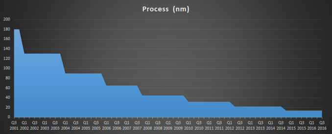
Looking forward, Intel is forecasting revenues for Q4 at $15.7 billion, plus or minus $500 million, and margins of 61%.
Intel has continued to diversify its portfolio, and has been building out other divisions to assist with growth while the PC market continues to decline, and while the Client Computing Group continues to be their largest division, they have had strong growth in other areas like the Data Center Group which had record revenue this quarter, and IoT which continues to grow quickly.
Source: Intel Investor Relations
↧
AMD Announces Q3 2016 Financial Results
Today AMD announced their third quarter earnings for the fiscal year 2016. Revenue was up to $1.307 billion, up 23% from a year ago. However their operating income and net income were not quite so lucky, with AMD showing an operating loss of $293 million for the quarter, compared to a $158 million operating loss a year ago, and net AMD showed a loss of $406 million, or $0.50 per share, compared to a net loss of $197 million, or $0.25 per share, a year ago.
| AMD Q3 2016 Financial Results (GAAP) | |||
| Q3'2016 | Q2'2016 | Q3'2015 | |
| Revenue | $1307M | $1027M | $1061M |
| Gross Margin | 5% | 31% | 23% |
| Operating Income | -$293M | -$8M | -$158M |
| Net Income | -$406M | +$69M | -$197M |
| Earnings Per Share | -$0.50 | $0.08 | -$0.25 |
AMD took a charge of $340 million this quarter for their sixth amendment to the wafer supply agreement with GlobalFoundries. This has been excluded in their Non-GAAP measures to show the core business, where they had the same $1.307 billion revenue, but showed an operating income of $70 million for the quarter, compared to an operating loss of $97 million a year ago. Non-GAAP net income for the quarter was $27 million, compared to a $136 million loss in Q3 2015.
| AMD Q3 2016 Financial Results (Non-GAAP) | |||
| Q3'2016 | Q2'2016 | Q3'2015 | |
| Revenue | $1307M | $1027M | $1061M |
| Gross Margin | 31% | 31% | 23% |
| Operating Income | $70M | $3M | -$97M |
| Net Income | $27M | -$40M | -$136M |
| Earnings Per Share | $0.03 | -$0.05 | -$0.17 |
Thanks to the charge, gross margin in GAAP terms was an abysmal 5% for the quarter, but Non-GAAP was 31%.
AMD’s Computing and Graphics segment had revenue of $472 million this quarter, which is up 11% from Q3 2015. Increased sales of GPUs are attributed to the gain, but the gain was offset by a drop in desktop processor sales, though they have seen an increase in sales of notebook processors. This segment continues to be unprofitable, having an operating loss of $66 million this quarter, but that is much better than the $181 million operating loss a year ago. Once again, GPU revenue has helped here tremendously. GPU average selling price (ASP) increased with higher channel and professional graphics ASPs. CPU ASP was flat year-over-year.
| AMD Q3 2016 Computing and Graphics | |||||
| Q3'2016 | Q2'2016 | Q3'2015 | |||
| Revenue | $472M | $435M | $424M | ||
| Operating Income | -$66M | -$81M | -$181M | ||
Enterprise, Embedded, and Semi-Custom continues to grow, and has easily surpassed the Computing and Graphics division, with revenues of $835 million, which is up 31% year-over-year. Semi-custom SoC sales continue to be the bright spot for AMD, with AMD have locked up both current generation consoles in the Xbox One, and PlayStation 4, and their refreshes in the Xbox One S and PlayStation 4 Pro, as well as the upcoming Xbox Project Scorpio. Best of all for AMD, this segment continues to be profitable, with an operating income of $136 million this quarter, up from $84 million a year ago.
| AMD Q3 2016 Enterprise, Embedded, and Semi-Custom | |||||
| Q3'2016 | Q2'2016 | Q3'2015 | |||
| Revenue | $835M | $592M | $637M | ||
| Operating Income | $136M | $84M | $84M | ||
AMD plunked the wafer agreement charge right into their All Other category, which had an operating loss of $363 million this quarter, compared to an $11 million loss last quarter, and a $61 million loss in Q3 2015.
AMD has seen success with its Polaris architecture in the GPU space, and they hope to see some success with their upcoming Zen CPU architecture, with their Summit Ridge desktop processor and a 32-core, 64-thread server product code named Naples.
Looking forward to next quarter, AMD expects revenues to decrease 18%, plus or minus 3%.
↧
AMD Releases Radeon Software Crimson Edition 16.10.2
![]()
We are now wading through the blockbuster season for the PC gaming industry. Consequently, the list of fixes is on the shorter side this time around, but AMD is adding official support for five titles coming out over the near future, with two games bundling in updated CrossFire profiles as well. (ed: So would this mean that Civ VI minus Battlefield 1 = 5 games?)
For bug fixes, after updating Radeon Software Crimson Edition 16.10.2 to driver version 16.40.2911, the driver no longer maintains elevated fan speed on select Radeon RX 400 cards after an application has been closed. Eyefinity group settings were not retained after driver upgrade when using CrossFire, this issue is now resolved. Next, Gears of War 4 will no longer hang when using high resolution and quality settings in some maps, and DX12 should now have less problems launching on some older CPUs that do not support the popcnt instruction.
On the newly supported games list this week we start with Battlefield 1, coming out this week with a new AMD CrossFire Profile update. There is also support for Sid Meier’s Civilization VI which will be released this week with a new CrossFire profile as well. Titanfall 2 made the roster though we won’t be seeing that game's release until next Friday the 28th. We also have some new VR experiences joining the party with the classic series Serious Sam and lastly, the incoming Eagle Flight VR.
As always, those interested in reading more or installing the updated hotfix drivers for AMD’s desktop, mobile, and integrated GPUs can find them either under the driver update section in Radeon Settings or on AMDs Radeon Software Crimson Edition download page.
↧